US $49.00
| Condition: |
New: A brand-new, unused, unopened, undamaged item in its original packaging (where packaging is
applicable). Packaging should be the same as what is found in a retail store, unless the item is handmade or was packaged by the manufacturer in non-retail packaging, such as an unprinted box or plastic bag. See the seller's listing for full details.
...
|
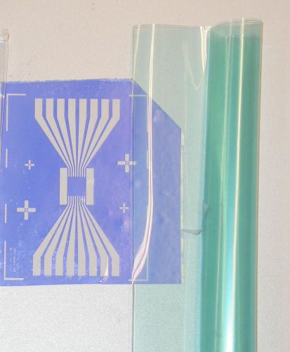
Brand | DuPont Riston |
| Model | FX-515 |
Directions
Similar products from Maintenance & Supporting Tools for Electronic Components
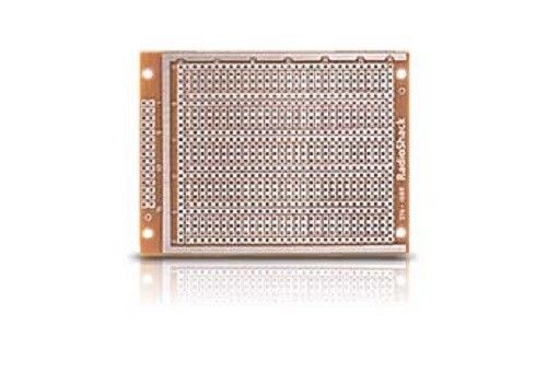
Universal Component PC Board with 780 Holes
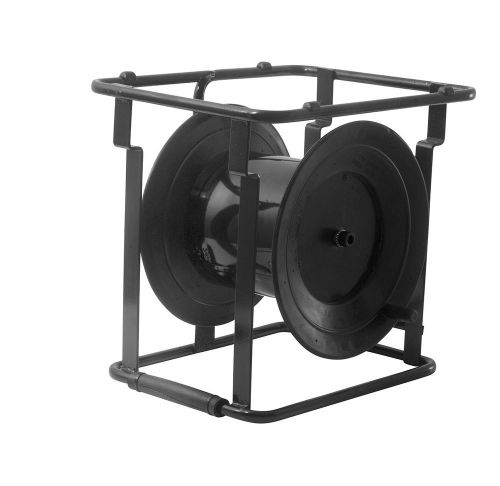
Portable, robust, for long cables, light, steel cable reel/drum
56T0250 Twin Industries Tw-E40-1020 Breadboard, Solderless, 830 Tie Points
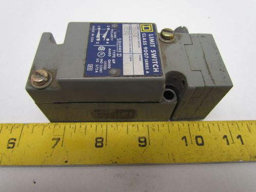
Square D C54B2 CO54 Limit Switch Class 9007 SeriesA
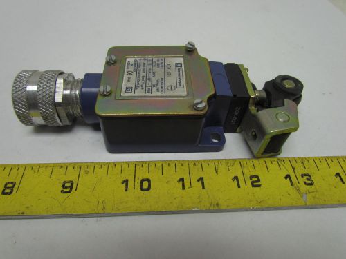
Telemecanique XCKL121 240V 3amp Limit Switch
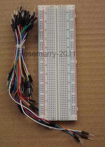
MB102 Breadboard 830 Points/65pcs Arduino Male/Male Solderless Breadboard Jumper
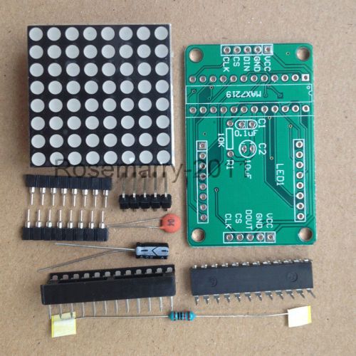
MAX7219 Dot matrix module MCU control Display module DIY kit for Arduino
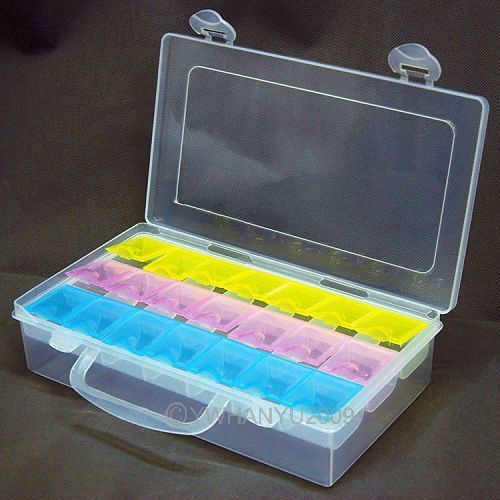
New Wholesale SMD SMT Electronic Components Storage Box, 21 Lattice/Blocks 82683
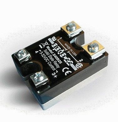
OPTO-22-120-240 VAC, 25 Amp, DC Control Solid State Relay (SSR) 3-32V DC CONTROL
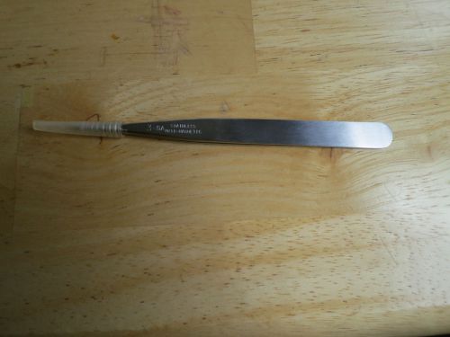
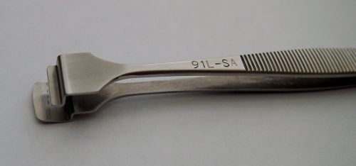
PRECISION TWEEZER ITALY VIOLA SIZE 3-SA STAINLESS STEEL - ANTI MAGNETIC
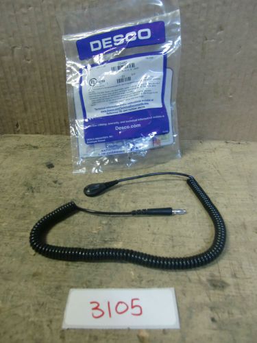
DESCO 2PK GROUNDING CORD BLACK 6" SERIES ESD STATIC CONTROL (3105)
Wafer Handling Tweezer Made In Switzerland
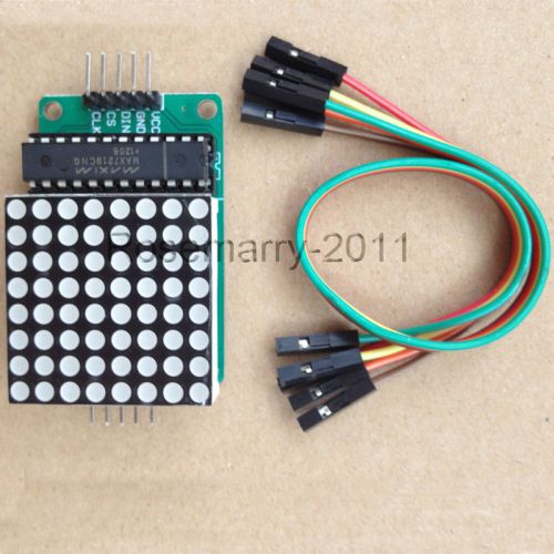
MAX7219 Dot matrix module MCU control Display module for Arduino W Dupond Cable
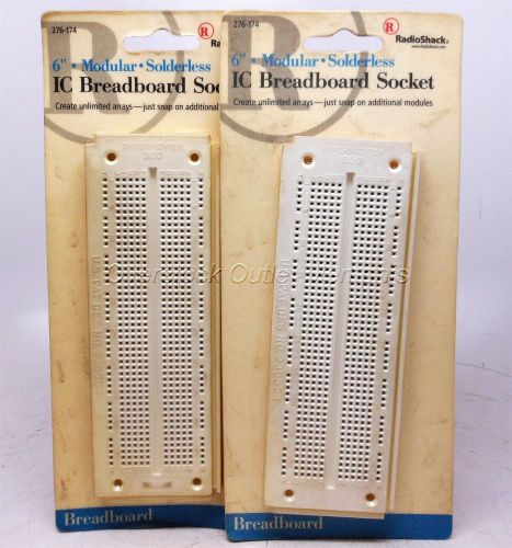
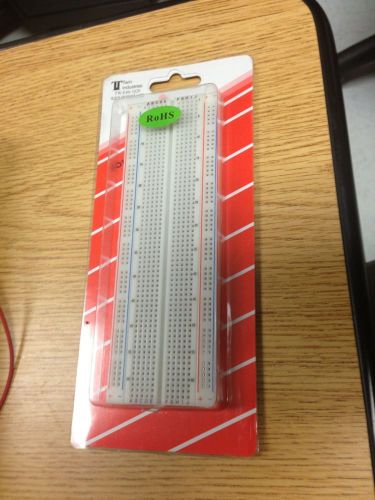
Two (2) RadioShack #276-174 6" Modular Solderless IC Breadboard Socket
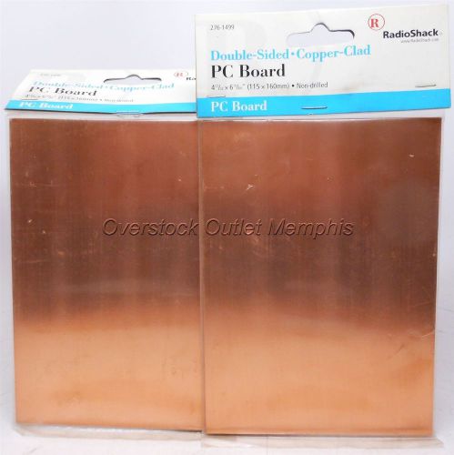
Two (2) RadioShack #276-1499 4"x6" Double-Sided Copper-Clad PC Boards
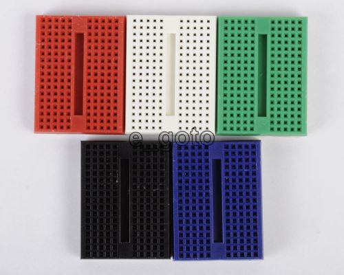
5pcs 5 colors Breadboard SYB-170 Solderless Prototype Tie-point for Arduino new
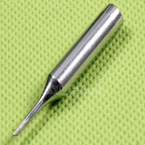
900M-T-1C Replaceable 936 Soldering Professional Solder Iron Tip
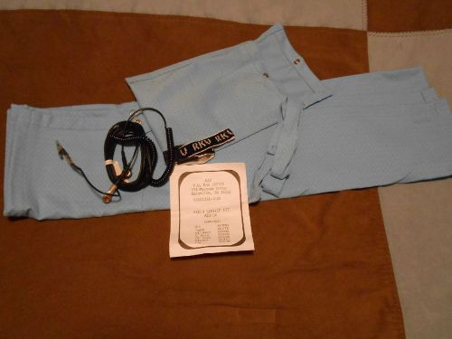
Anti Static Field Service Kit with Mat, Adjustable Band, 6' and 10' Cords
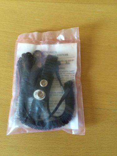
Semtronics wrist band grounding system SE4000 (NIB)
SURFACE MOUNT LED LAMP BY FAIRCHILD SEMICONDUCTOR
People who viewed this item also vieved
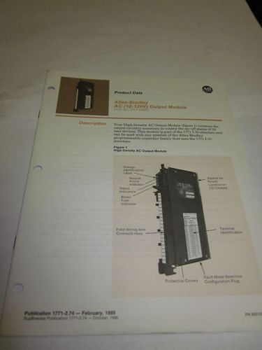
Allen Bradley Output Module Product Data Manual, Used
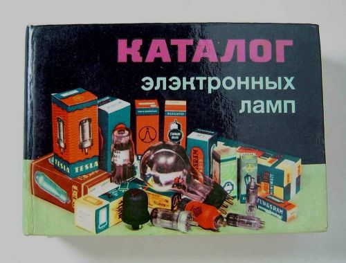
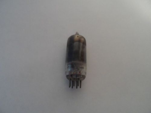
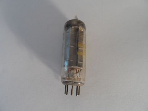
Tube Catalogue Reference Book Russian Electronic Radio Old Vintage Lamp Czech
Norlux 132589 LED Driver 120-277VAC 58vdc 45W Max Dimmable 1-10v Dry or Damp Loc
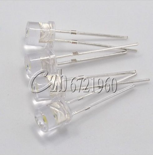
500PCS 2Pin 5MM Flat Top White LED Wide Angle Flat Head Light Lamp
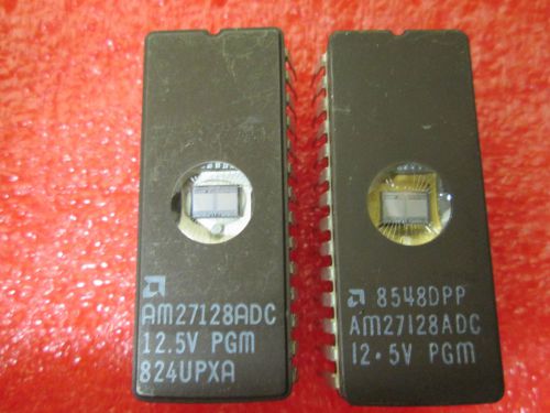
6 PSC AM27128 ADC 27128 EPROM VINTAGE DIP 28 PIN 128K (16K x8) NMOS UV
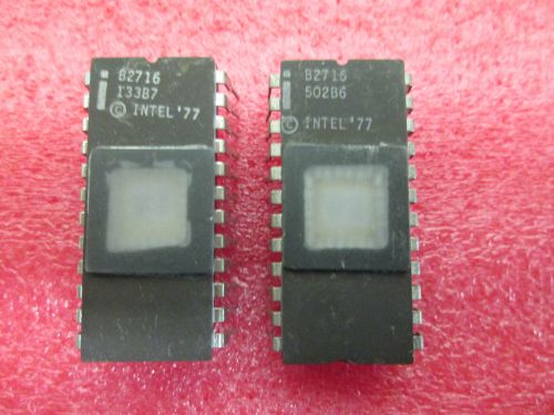
INTEL EPROM B2716 VINTAGE IC 16K (2KX8) CERAMIC DIP PACK 24 PIN
15-PCS MICREL MIC29501-5.0WU 2950150 MIC2950150WU
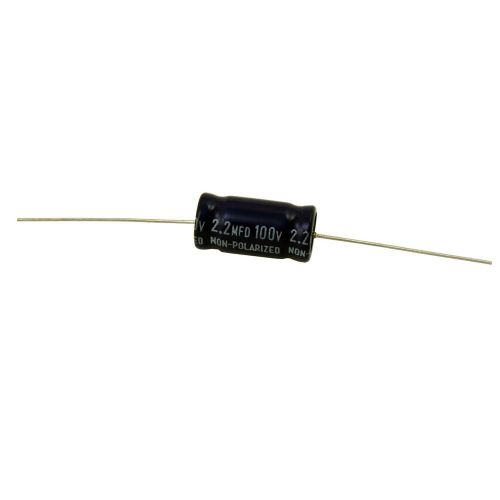
Set of 10 (2.2 mfd uF Axial Electrolytic non Polar Capacitor 100 V)
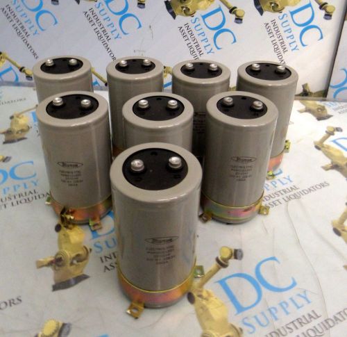
MARCON PWM2A2A223 22000µF ELECTROLYTIC CAPACITOR LOT OF 8
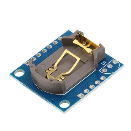
RTC I2C DS1307 AT24C32 Real Time Clock Module For Arduino AVR ARM PIC 51 ARM HC
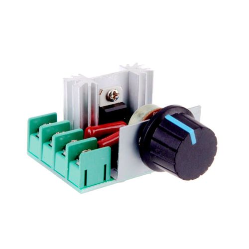
1Pcs 25A 220V 2000W Speed Controller SCR Voltage Regulator Dimmers Thermostat
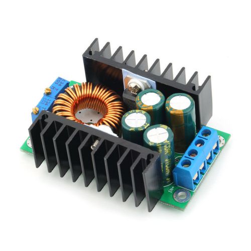
7-32V to 0.8-28V 12A DC-DC CC CV Buck Converter Step-down Power Supply Module
By clicking "Accept All Cookies", you agree to the storing of cookies on your device to enhance site navigation, analyze site usage, and assist in our marketing efforts.
Accept All Cookies