US $567
Directions
Similar products from Other Semiconductors & Active Components
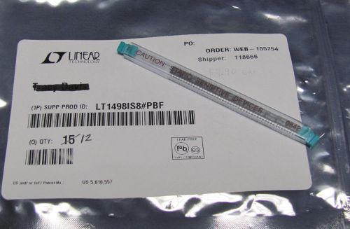
12pcs - LT1498IS8, Linear Technology Op-Amp, 10Mhz, Rail-to-Rail, SO-8
USED Lamp Driver AMI PART 0190-17464 P1191D
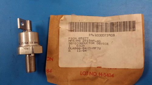
5961-00-007-3908 MFR/PN 2515AFLAG SEMICONDUCTOR DEVICE
1 LOT OF 1450 ON SEMICONDUCTOR MC74HC4053ADTR2G NEW
1 LOT OF 900 DIODS INC B260-13-F NEW
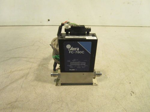
Aera FC-780C Mass Flow Controller 21J0489 50SCCM
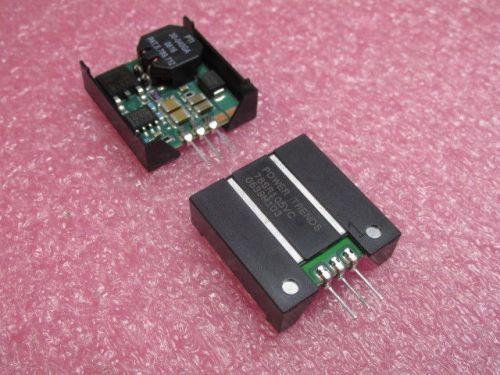
50 PCS POWER TRENDS 78SR105VC POWER MODULES
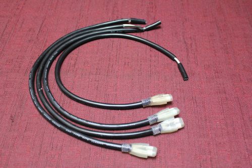
Marl International 066-000-00-50 LED pathlighting power cord New
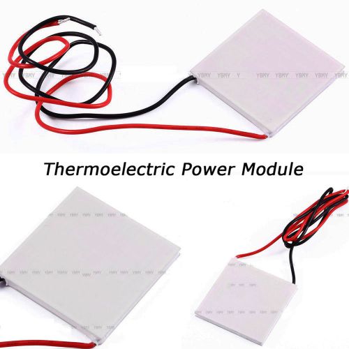
New Thermoelectric Power Generator Peltier Module TEG 40*40mm High Temperature
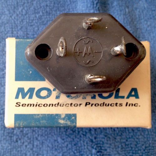
MOTOROLA SEMICONDUCTOR TYPE MDA 952-1
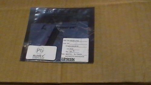
Lot of 8 Hittite Microwave HMC601LP4(E) Logarithmic Detector/Controller

MICROCHIP PIC16F, PICDEM 2 PLUS, DEMO BOARD

General Electric GE C152N Diode Stud Attached

IR 72RA120 Diode Stud Attached

Allen Bradley 800E-3DL3X10 Module with Latch

Philips ECG 5710 Thyristor Module
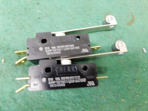
2 CHERRY LONG HINGE LEVER SNAP LIMIT SWITCH 15A 125 OR 250VAC 3/4 HP 1-1/2 HP

10x MRF648 NPN SILICON RF POWER TRANSISTOR

qty 1 SEEQ DQ5133-350 Eproms ic chips cf2-17

qty 1 SEEQ DQ5133-200 Eproms ic chip cf2-17
People who viewed this item also vieved

NC7SZ14P5X TinyLogic UHS Inverter Schmitt Trigger input, SC70-5, Qty.10

Toshiba 8V/30mA LDO Regulator TA78DS08F, SOT-89, Qty.10

LP339M NSC Ultra Low Power SOIC-14, Lot of 25 pcs, multiple lots available

Synergy SY100S811ZC Syngle Supply 1:9 PECL/TTL-to-PECL SY100S811
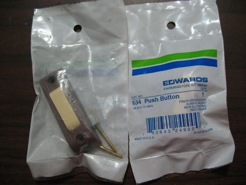
New Lot of 2 Edwards 634 Door Bell Push Buttons
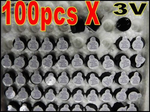
100PCS Active Buzzer Magnetic Long Continous Beep Tone Alarm Ringer 3V 12mm NEW
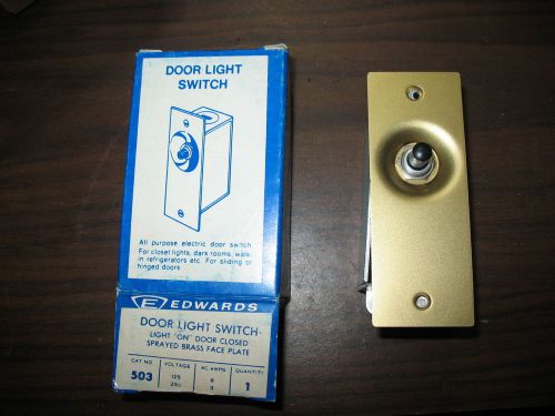
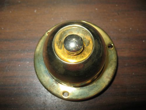
New Edwards 503 Door Light Switch with Sprayed Brass Faceplate
New Tork Alert TA1786B Weatherproof Brass Pushbutton - Missing Screws
Rectifiers 200V 1A Fast (1000 pieces)
Rectifiers Standard 600V 2A (1000 pieces)
Diodes - General Purpose, Power, Switching 250mA 75V (1000 pieces)
Diodes - General Purpose, Power, Switching vR/100V Io/150mA (1000 pieces)
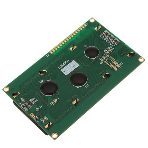
2pcs 20X4 Character LCD Module Display Blue Backlight Xmas Gift
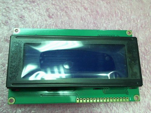
1PIC 2004A 20x4 Character LCD Display Module 5V Blue Blacklight
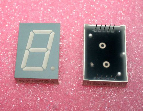
GREEN SINGLE DIGIT 1" LED SA10-21GWA - Lot of 10 (SA10_21GWA)
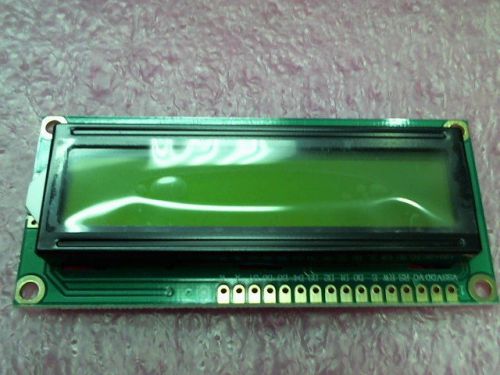
1602 162 16x2 Character LCD Display Module HD44780 Controller Yellow Blacklight
VISHAY SEMICONDUCTOR VS-26MB20A BRIDGE RECT MOD, 1PH, 25A, 200V, QC (1 piece)
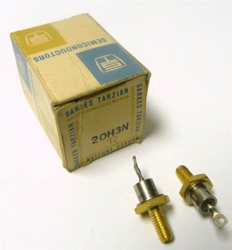
BRAND NEW SARKES TARZIEN RECTIFIER MODEL 20H3N (BOX OF 2)
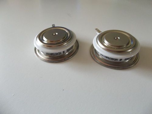
Pair of Westcode SCR # N0465WN160
VISHAY SEMICONDUCTOR VS-26MB120A BRIDGE RECT MOD, 1PH, 25A 1.2KV, QC (1 piece)

5x 2SA1943 & 5x 2SC5200 TOSHIBA High Power Audio Transistor. SKU83171C

SIR164DP-T1-GE3 SIR164DP VISHAY MOSFET N-CH 30V 50A PPAK SO-8 Q'TY:10PCS/LOT

OZ9950GN_LCDM Inverter Controller_O2Micro Q'TY:2PCS/LOT

RLZTE-11 18B ROHM RLZTE-1118B DIODE ZENER 17.3V 500MW LLDS Q'TY:100PCS/LOT
By clicking "Accept All Cookies", you agree to the storing of cookies on your device to enhance site navigation, analyze site usage, and assist in our marketing efforts.
Accept All Cookies