US $49.99
| Condition: |
New: A brand-new, unused, unopened, undamaged item in its original packaging (where packaging is
applicable). Packaging should be the same as what is found in a retail store, unless the item is handmade or was packaged by the manufacturer in non-retail packaging, such as an unprinted box or plastic bag. See the seller's listing for full details.
...
|
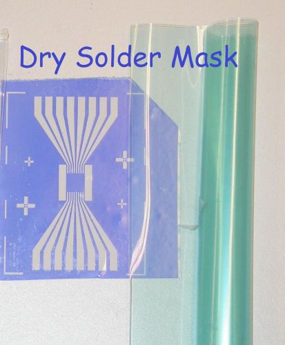
Brand | Dynamask |
| Model | 5000 |
Directions
Similar products from Maintenance & Supporting Tools for Electronic Components
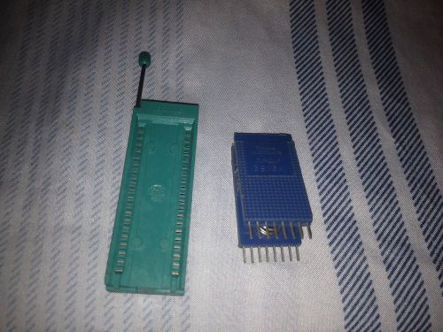
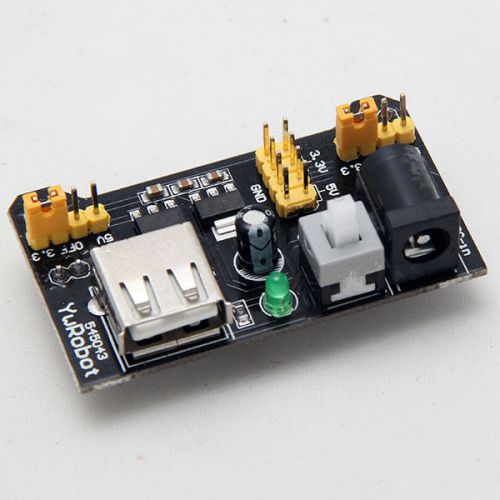
Textools Test Socket - 40 pins and Pomona Dip Clip 3196A, 16 pins - VGC
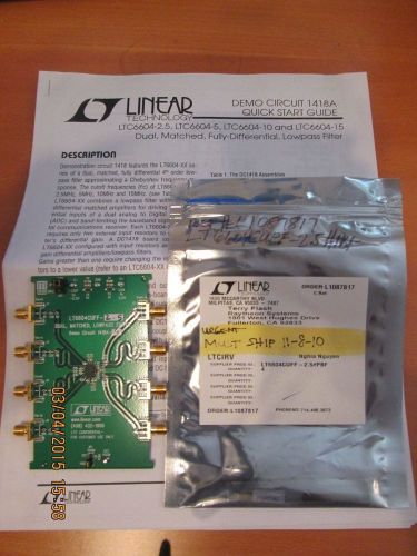
Linear Technology LT6604 Eval Board. Dual 2.5MHz Lowpass Filter, Amateur Radio
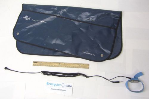
Spirent Communications PVC Anti-Static Mat 23x23" + Wrist Strap 53579
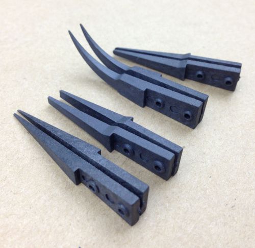
Anti-Acid Precision Tweezers 4set style Head
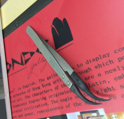
Anti-Acid steel Pointed Tweezer Fine tip Curved BMS-17 WEITUS
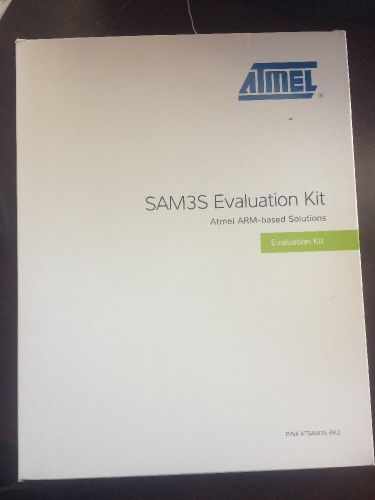
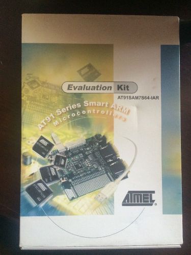
Atmel AT91 Series Smart ARM Eval
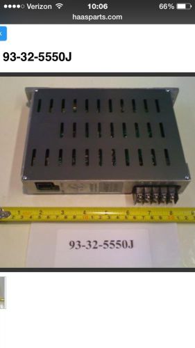
HAAS 30 Amp Servo amplifier 93-32-5550J. New in sealed box.
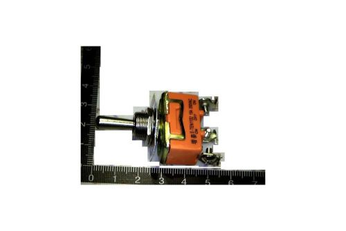
2 Pieces 3 Pins 3 Position Toggle Switch E-TEN1122 15A 250VAC

Amico Plastic 24 Compartments Electronic Components Jewelry Storage Box Case Con
Blue High Voltage Anti-Static Static Discharger Key Ring
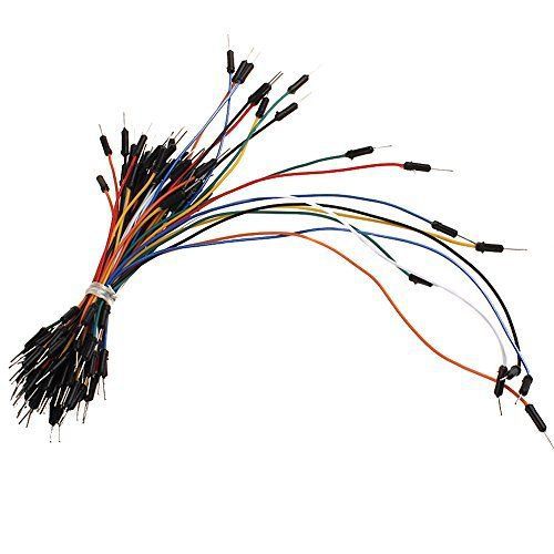
EUBUY Solderless Flexible Breadboard Jumper Wires Cable Kits Male To Male (100)
10 pieces Multifunction Switch 4 pins position: 2 on and 1 off 214A
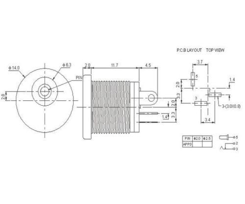
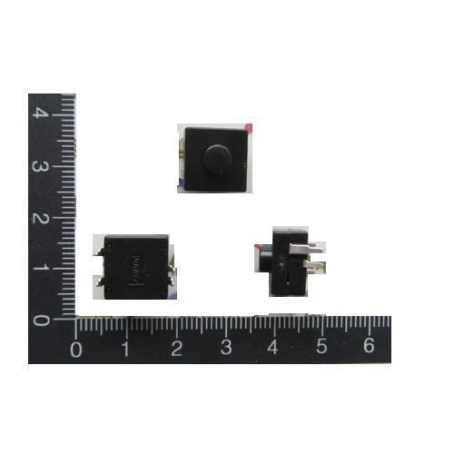
5 pieces DC-022 DIA 12MM Power Jack FOR 2.0mm socket
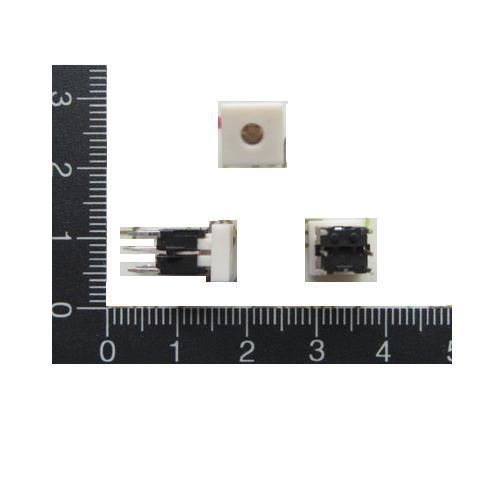
10 pieces 6 * 6 * 9MM Red Light Hat Micro Touch Button Switch
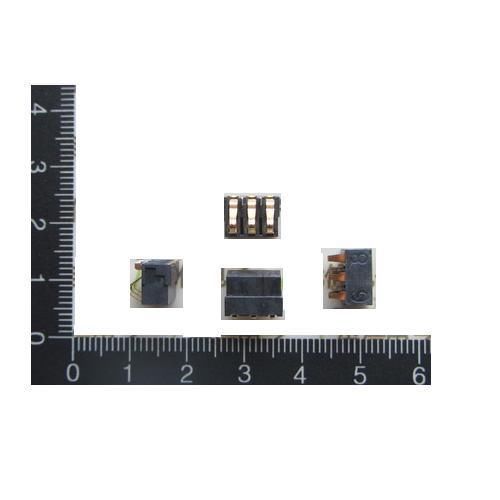
10 pieces 6*8 cell battery holder connector gold-plated phosphor bronze shrapnel
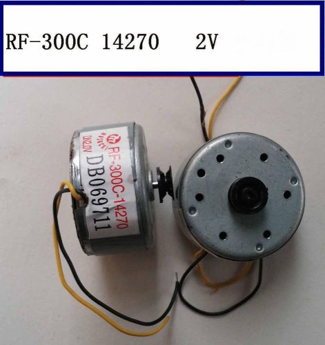
2 pieces RF-300C-14270 MOTOR WITH small Pulley plate 2-3V diameter 2.5mm height
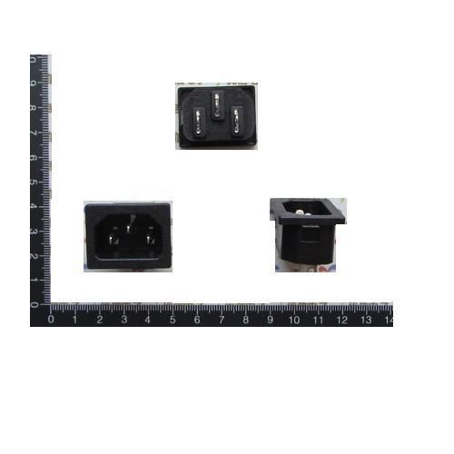
10 pieces Power Connector Socket Jack ST-A01-003J/250V-10A Copper pins
People who viewed this item also vieved
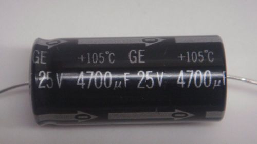
50pcs Panasonic GE 4700uF 25v 105C Axial Electrolytic Capacitor
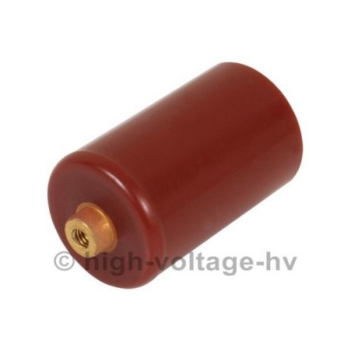
Doorknob Capacitor, High Voltage Ceramic Capacitor 50kV 20pF
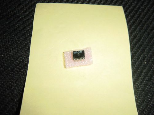
NEW 221-132 ZENITH INTEGRATED CIRCUIT ECG863, NTE863
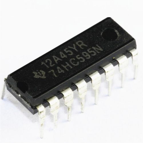
10PCS IC 74HC595 74595 SN74HC595N 8-Bit Shift Register DIP-16
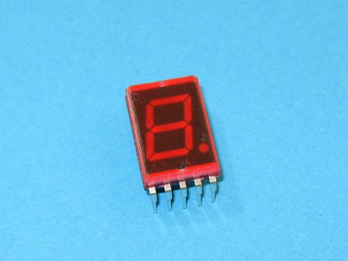
NEC SN713B , 0.45inch 7-segment Red LED Display Common Anode
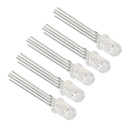
50Pcs LED RGB common cathode 4-PINS F5 5MM Super Bright Bulb Lamp new
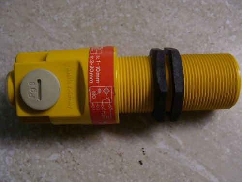
turck elektronik feinbau 220-30 220-40
NEW OPTICAL LASER LENS for HARMAN KARDON CDR-2 / CDR-20 PLAYER
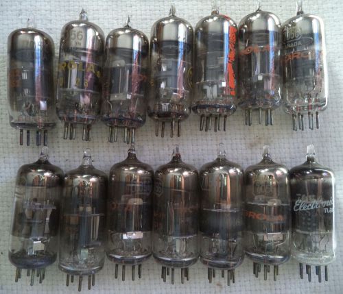
(14) Used 7056 Sharp Cutoff Pentode for Use in Mobile Equipment N/R
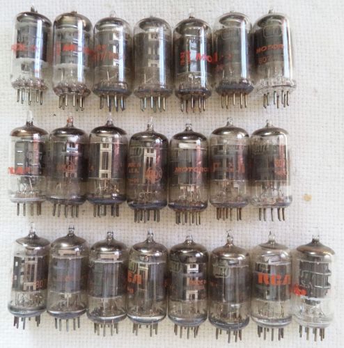
(22) Used 8077 Power Pentode Tube for Use in Mobile Equipment as Amp or Osc N/R
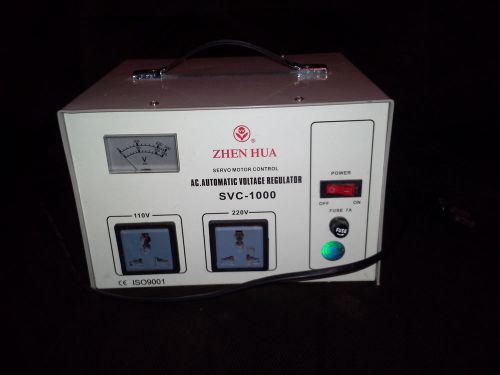
Zhen Hua SVC-1000 Alternating Current Automatic 110 to 220 Voltage Regulator
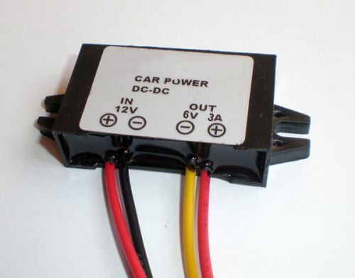
Industry Grade DC 12V To DC 6V 3A Step-Down Converter


Intermediate Robot Building PDF
By clicking "Accept All Cookies", you agree to the storing of cookies on your device to enhance site navigation, analyze site usage, and assist in our marketing efforts.
Accept All Cookies