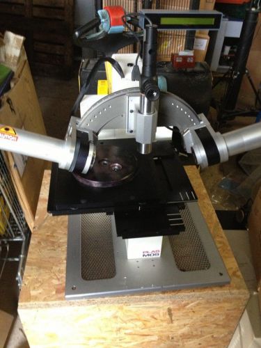
US $6,900.00
Directions
Similar products from Inspection Tools & Machinery
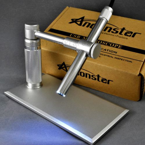
2MP USB Digital Microscope Endoscope Camera PCB Circuit Board Inspection tool US
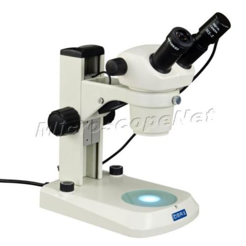
20X-40X Binocular Stereo Microscope with USB Digital Camera and Dual LED Lights
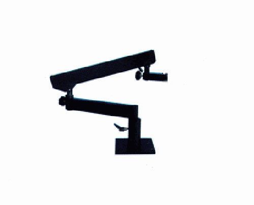
MICROSCOPE ARTICULATING ARM ON TABLE MOUNT
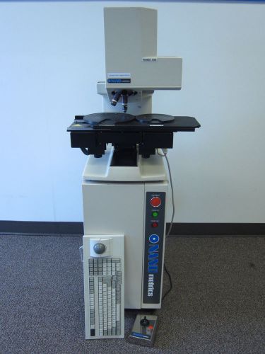
NANOSPEC NANO 6100 AUTOMATED FILM THICKNESS MEASUREMENT SYSTEM NANOMETRICS
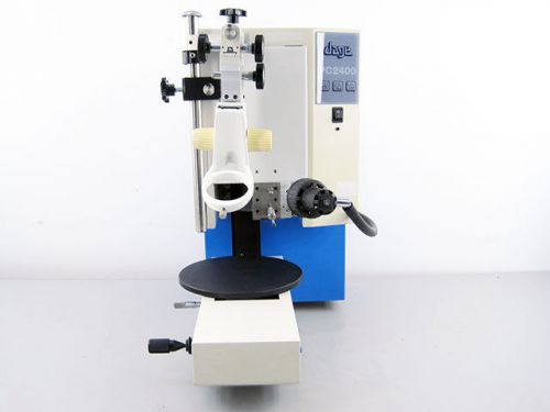
DAGE PC2400 WIRE PULL BALL SHEAR MICRO BOND TESTER
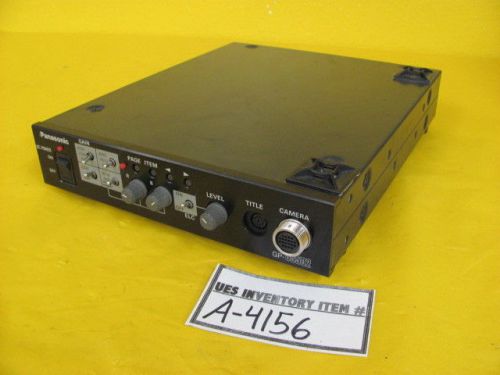
Panasonic GP-US502 Camera Control Unit Z-E115-01 working
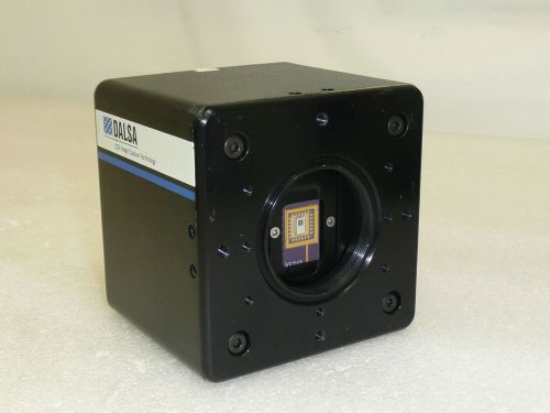
Dalsa CA-D1-0128A-STDN CCD Camera 128x128
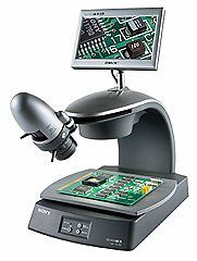
Sony Technolook TW-TL10S Video Microscope
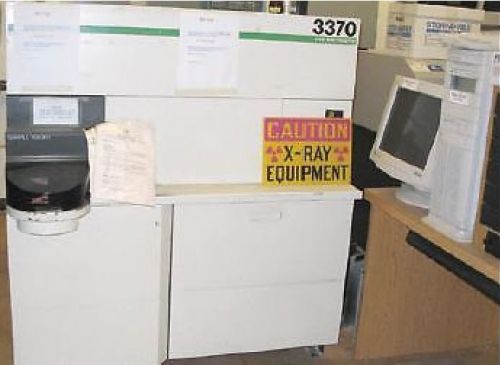
Rigaku 3370 X-Ray Spectrometer SEQUENTIAL XRF wXRF wdxrf Minerology elemental
Philips Assembleon ACM Verification Set 5322 395 10689
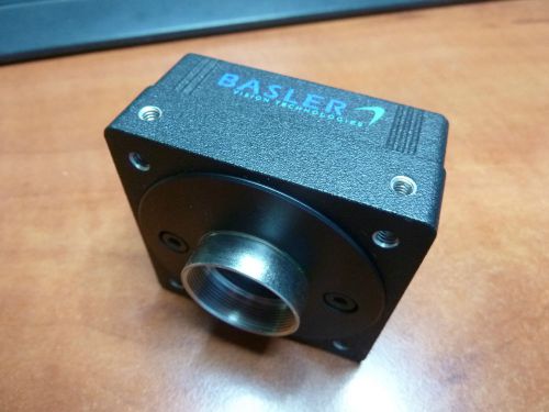
BASLER VISION TECHNOLOGIES MACHINE VISION CAMERA NOT COMPLETE
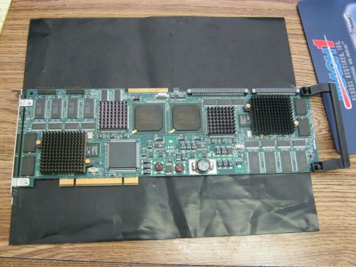
Matrox Gen/Pro: 925-0101 Board. GPG4N/400/256/2. PN: GPG4N/400/256/2. Rev.A<
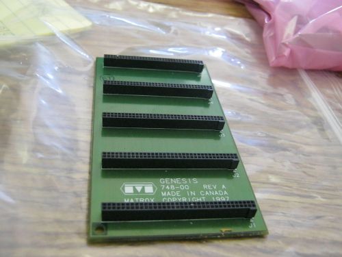
Matrox Genisis: 748-00 Interconnect Board. GEN-BUS/5. PN: GEM-BUS/5. Rev. A<

Matrox Genisis: 749-00 Interconnect Board. Rev. A<

DIALIGHT MAX RATING 75W, 125V LAMP SOCKET 250-8738-14-504 *NEW, SEALED*
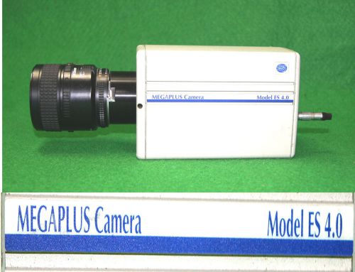
MEGAPLUS High Resolution Camera Model ES 4.0
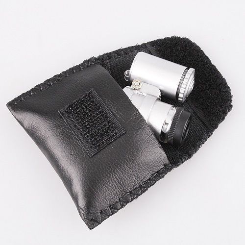
45X Mini Pocket 2LED Light Microscope Magnifier Jeweler Loupe With Leather Pouch
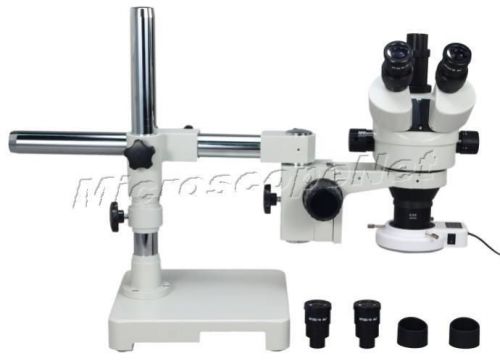
Boom Stand Zoom Stereo Microscope 3.5x-90X 54 LED Light
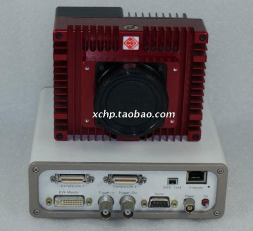
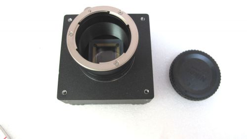
ONE MEGAPLUS II EC11000 Full 35mm 11 megapixel CCD VISION CAMERA
People who viewed this item also vieved
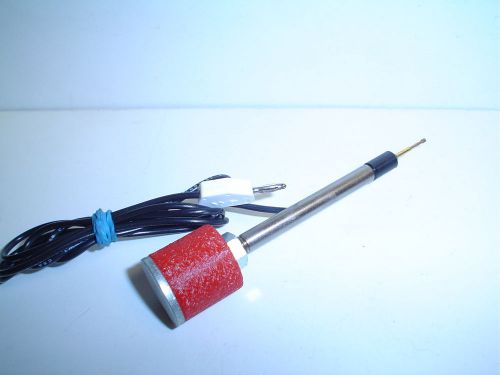
Seica PCB Test Probe Assembly with Spring Finger
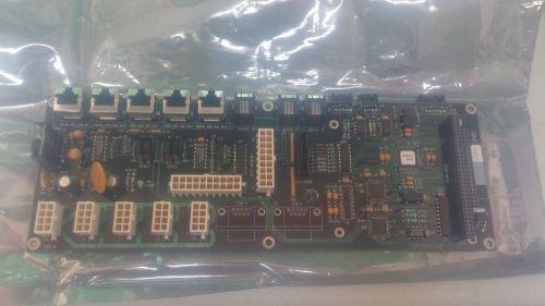
PRI AUTOMATION AUTO I/O MOTHERBOARD PCB 70018849 REV F WORKING
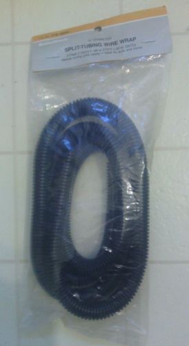
RadioShack 278-1624A Tubing, Split Wire Wrap, 5 feet (1.52cm) 1/2" diameter
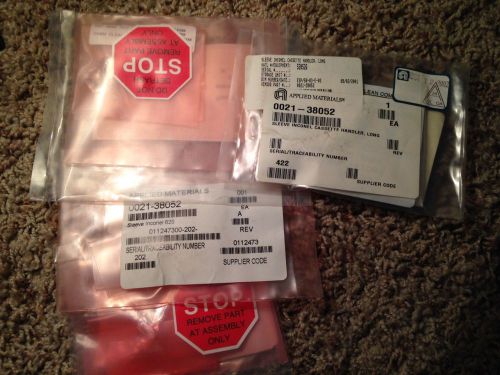
AMAT 0021-38052 SLEEVE INCONEL CASSETTE HANDLER, LONG
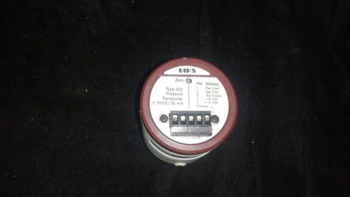
MKS BARATRON 622A12TAE PRESSURE TRANSDUCER 15 VDC-35 mA
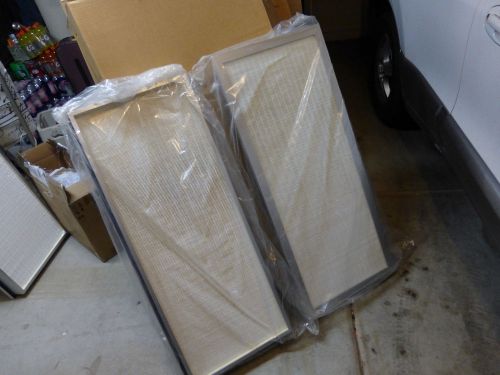
2 Camfil Farr Megalam Panel HEPA Filter 855029464 P5-17.37-41.37-4-41-VU-00-00-0
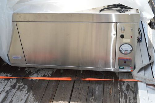
Laminar Flow Inc VLFU Stainless Portable Clean Room Cleanroom booth 42"x72"
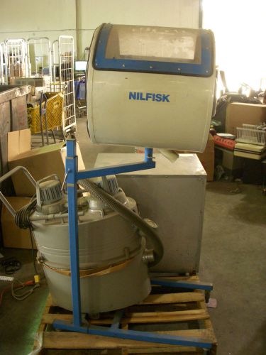
Nilfisk GS 82 Industrial Canister Portable Vacuum Cleaner with gloved chamber
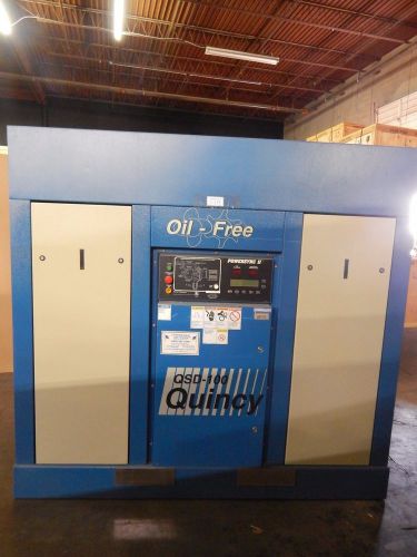
Quincy QSD-100 Oil Free Air Compressor Power Sync II MQSD100WA26A untested as is
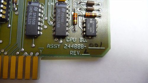
Electroglas CPU board assy 244888-001 2 REV L, D AND M . THERE ARE 4 BOARDS.
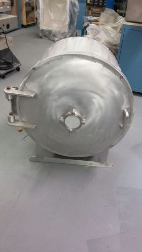
VACUUM CHAMBER 29" ID x 20" DEEP
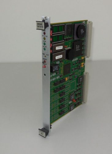
Motorola MVME 147-010 64-W5892B01B rev B 01-W3964B21D use on Noran instruments
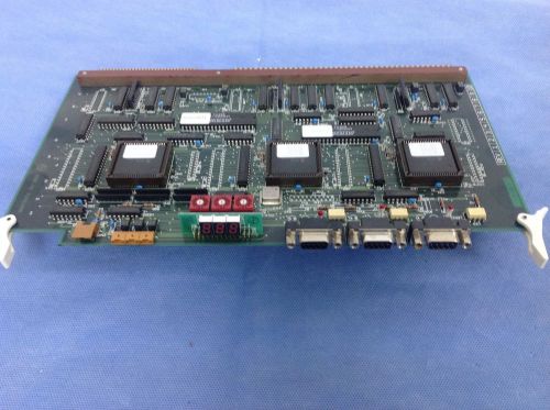
Kokusai Vertron D1E01300B Control Board SIOB/A2
By clicking "Accept All Cookies", you agree to the storing of cookies on your device to enhance site navigation, analyze site usage, and assist in our marketing efforts.
Accept All Cookies