


US $4.90
Directions
Similar products from PCB boards & Kits
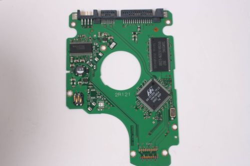
SAMSUNG HM160HI /D 160GB SATA 2,5 HARD DRIVE / PCB (CIRCUIT BOARD) ONLY FOR DATA
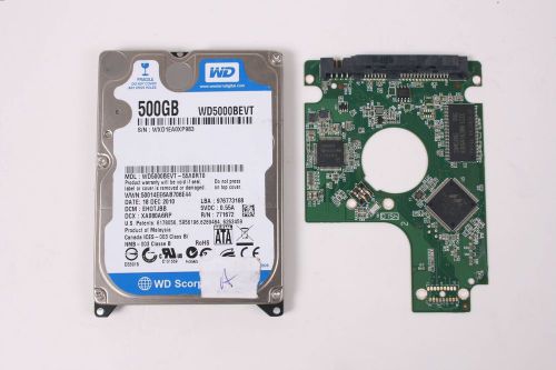
WD WD500BEVT-55A0RT0 500GB 2,5 SATA HARD DRIVE / PCB (CIRCUIT BOARD) ONLY FOR DA
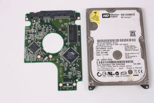
WD WD1200BEVS-00LAT0 120GB 2,5 SATA HARD DRIVE / PCB (CIRCUIT BOARD) ONLY FOR DA
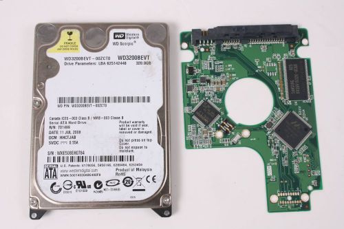
WD WD3200BEVT-00ZT0 320GB 2,5 SATA HARD DRIVE / PCB (CIRCUIT BOARD) ONLY FOR DAT
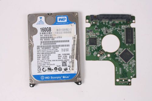
WD WD1600BEVT-60ZCT1 160GB 2,5 SATA HARD DRIVE / PCB (CIRCUIT BOARD) ONLY FOR DA
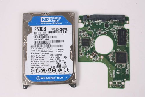
WD WD2500BEVT-22ZAT0 250GB 2,5 SATA HARD DRIVE / PCB (CIRCUIT BOARD) ONLY FOR DA
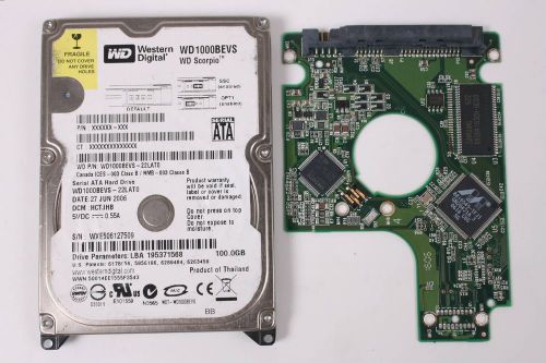
WD WD1000BEVS-22LAT0 100GB 2,5 SATA HARD DRIVE / PCB (CIRCUIT BOARD) ONLY FOR DA
WD WD2500BEVT-75A23T0 250GB 2,5 SATA HARD DRIVE / PCB (CIRCUIT BOARD) ONLY FOR D
WD WD1600BEVT-22A23T0 160GB 2,5 SATA HARD DRIVE / PCB (CIRCUIT BOARD) ONLY FOR D
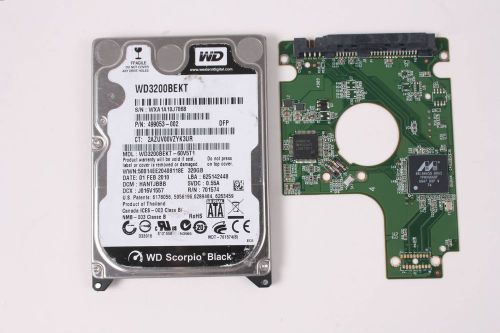
WD WD3200BEKT-60V5T1 320GB 2,5 SATA HARD DRIVE / PCB (CIRCUIT BOARD) ONLY FOR DA
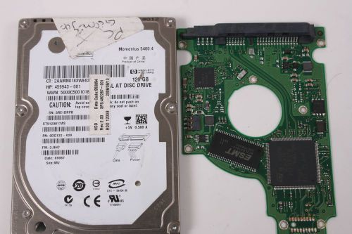
SEAGATE ST9120817AS 120GB 2,5 SATA HARD DRIVE / PCB (CIRCUIT BOARD) ONLY FOR DAT
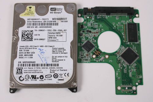
WD WD1600BEVT-75ZCT1 160GB 2,5 SATA HARD DRIVE / PCB (CIRCUIT BOARD) ONLY FOR DA
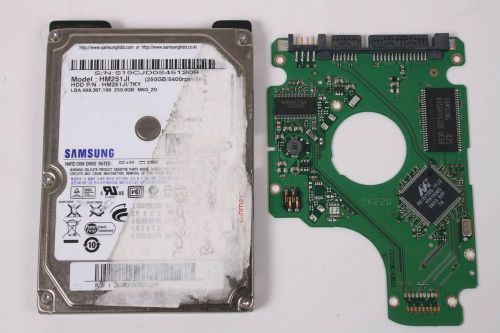
SAMSUNG HM251JI /TKY 250GB 2,5 SATA HARD DRIVE / PCB (CIRCUIT BOARD) ONLY FOR DA
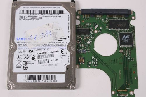
SAMSUNG HM250HI /LMC 250GB 2,5 SATA HARD DRIVE / PCB (CIRCUIT BOARD) ONLY FOR DA
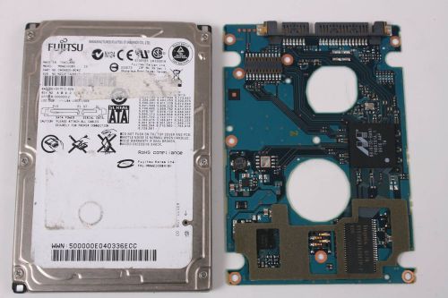
FUJITSU MHW2100BH 200GB 2,5 SATA HARD DRIVE / PCB (CIRCUIT BOARD) ONLY FOR DATA
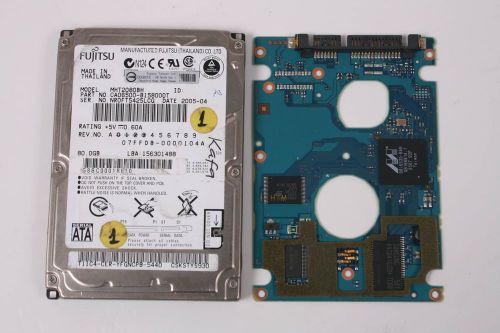
FUJITSU MHT2080BH 80GB 2,5 SATA HARD DRIVE / PCB (CIRCUIT BOARD) ONLY FOR DATA
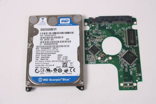
WD WD2500BEVT-60ZCT1 250GB 2,5 SATA HARD DRIVE / PCB (CIRCUIT BOARD) ONLY FOR DA
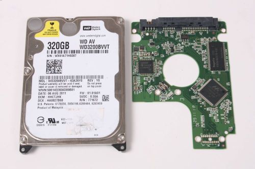
WD WD3200BVVT-63A26Y0 320GB 2,5 SATA HARD DRIVE / PCB (CIRCUIT BOARD) ONLY FOR D
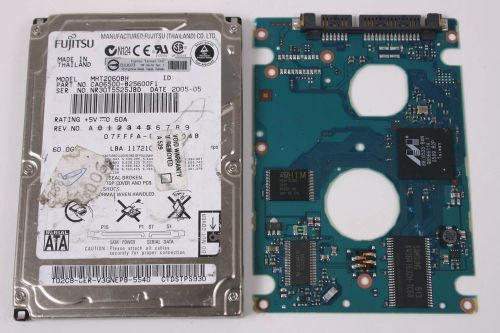
FUJITSU MHT2060BH 60GB 2,5 SATA HARD DRIVE / PCB (CIRCUIT BOARD) ONLY FOR DATA
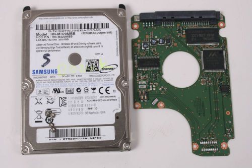
SAMSUNG HN-M320MBB 320GB 2,5 SATA HARD DRIVE / PCB (CIRCUIT BOARD) ONLY FOR DATA
People who viewed this item also vieved
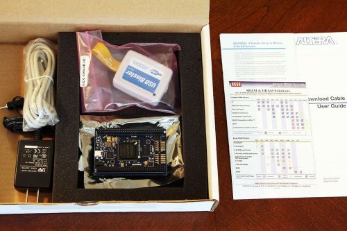
Professional Altera Cyclone IV Developers Kit with NIOS II
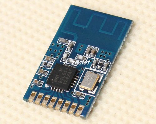
2.4G nRF24L01+ RFID Wireless Transmission Module 2.4GHz 2dBm 1mW Perfect
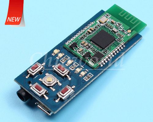
XS3868 Wireless Bluetooth Module Stereo Audio Module with Shield new
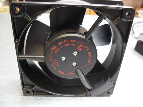
ebm - W2G107-AD05-12 - 48v DC 36-56v Axial Fan, Compact, Steel, NEW free ship
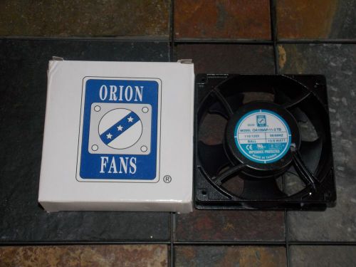
Orion Cooling Fan Rare OA109AP-11-3 OA109AP-11-3TB 110/120V 50/60HZ - New in Box
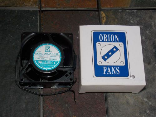
Orion Cooling Fan Rare OA80AP-11-1 OA80AP-11-1WB 115VAC 50/60HZ - New in Box
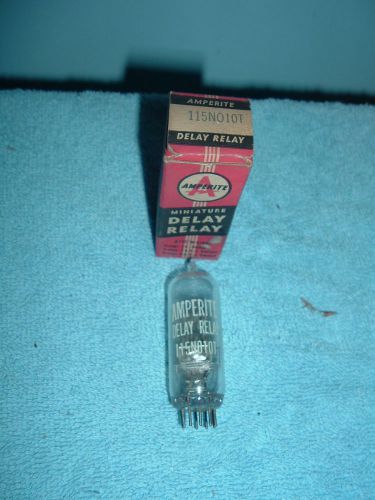
Vintage Amperite Type 115N010T Delay Relay Electronic Tube New Old Stock USA
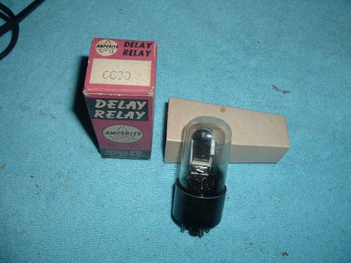
Vintage Amperite Type 6C90 Delay Relay Electronic Tube New Old Stock Made in USA
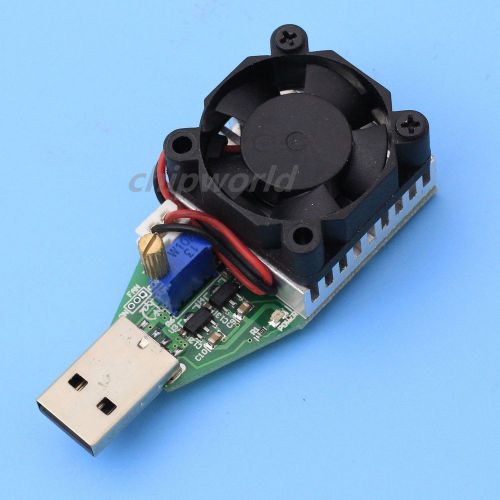
USB DC Electronic Load Module 15W 3A Steady Adjustable USB Discharger
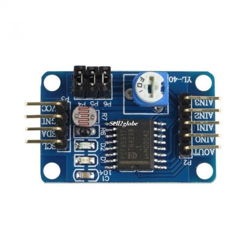
PCF8591 AD/DA Converter Module Analog To Digital Conversion for Arduino+Cable G8
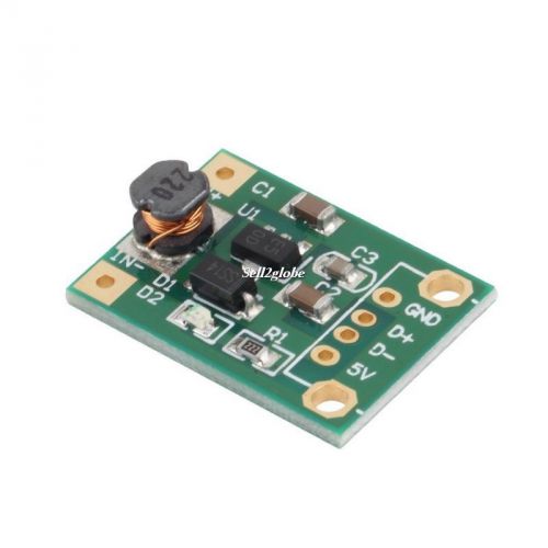
DC-DC Boost Converter Step Up Module 1-5V to 5V 500mA Power Module New G8
AMS1117 DC/DC Step-Down Voltage Regulator Adapter Power Supply Module G8
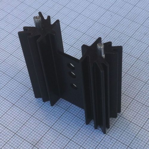
HEATSINKS FOR TO-220, TO-202 (4 PCS)
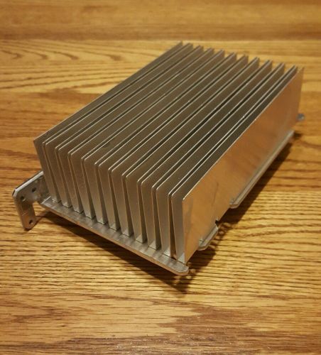
22 Fin Aluminum Heat Sink Used APPROX 4 7/8" X 7 5/8" - SHIPS FREE
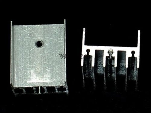
2pcs aluminum heat sink 25x24x16mm ic radiator for tda7294/l298 #268329
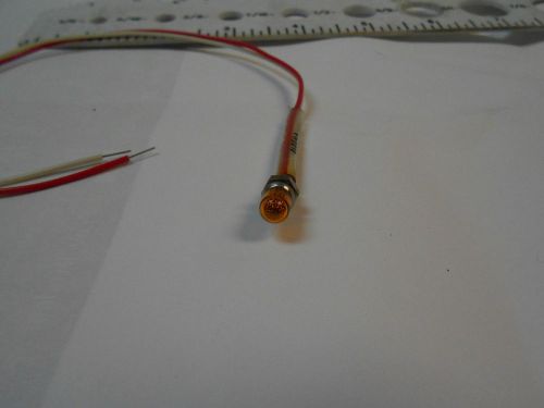
JM9152-003-810AC AMBER LIGHT DIODE PREWIRE 5" 2.8VAC NEW OLD STOCK

New 2PCS Universal Motorcycle 12 LED Front Turn Signal Blinker Indicators Light
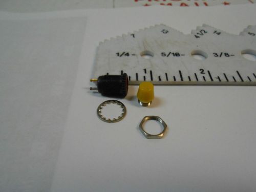
5160-458&160A MINIATURE LAMP AMBER -HOLE .31/LENTH .84/DIA .375 BULB T-1 NOS
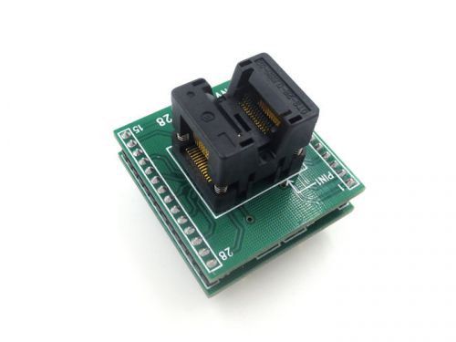
SSOP28 TSSOP28 OTS-28-0.635-02 IC Test Burn-in Socket Programming Adapter
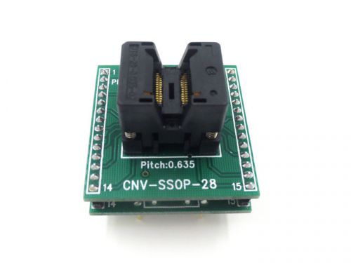
SSOP28 TSSOP28 IC Test Burn-in Socket Programming Adapter Pitch 0.635mm
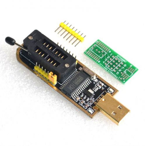
2pcs CH341A programmer USB motherboard routing BIOS LCD FLASH 2425 burner NEW
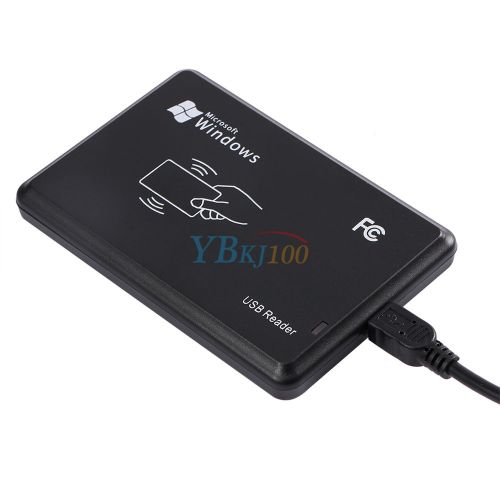
USB RFID Contactless Proximity Smart IC Card Reader Sensor USB Reader 13.56MHZ

NEW UTC Fire & Security 430083501 Magnetic Stripe Reader with keypad

New Handheld RFID ID Card Copier/ Reader/Writer 6 Writable Tags/6 Cards KG
By clicking "Accept All Cookies", you agree to the storing of cookies on your device to enhance site navigation, analyze site usage, and assist in our marketing efforts.
Accept All Cookies