


US $199.00
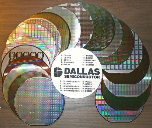
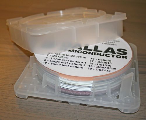
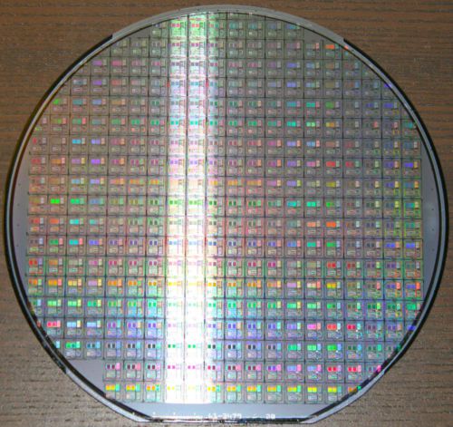
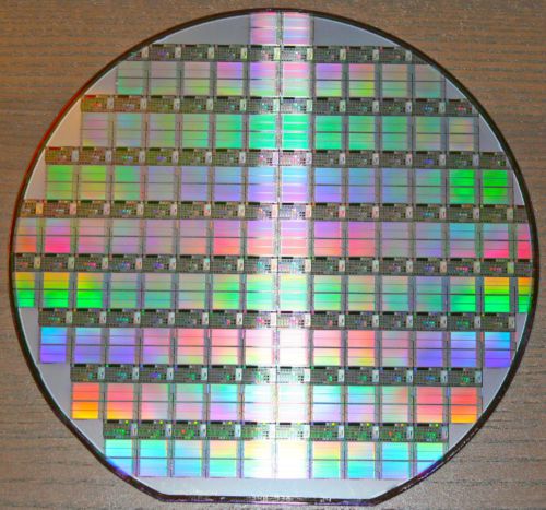
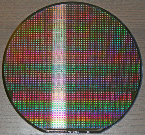
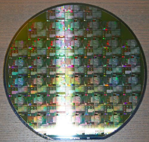
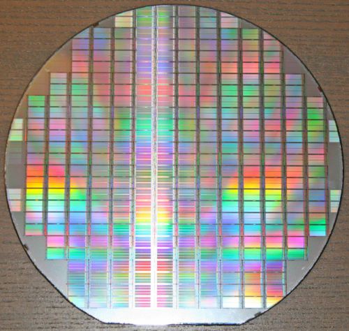
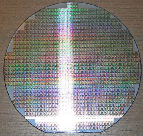
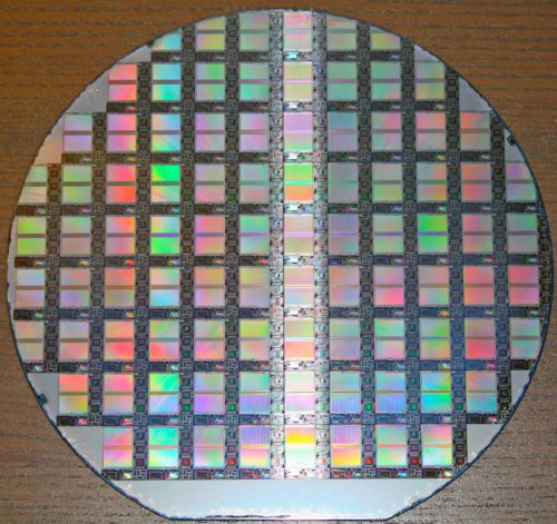
| “Wafers are physically pristine, with possible minor blemish or scratches from handling. The designs on the wafers are not functional and the lot is sold for education purposes only.” |
| Brand | Dallas Semiconductor |
| Country/Region of Manufacture | United States |
Directions
Similar products from Other Electronic Components & Spare Parts
Banner USCD-1T3 USCD1T3 Micro-Screen Control Box
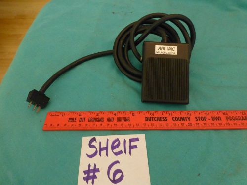
air vac engineering foot control pedal
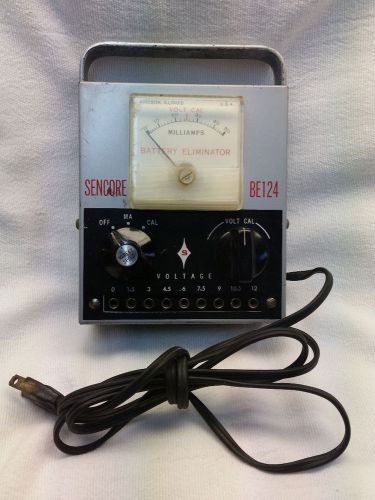
Vintage Sencore BE 124 Battery Eliminator Working Unit
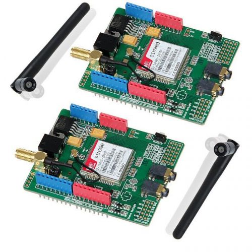
2pcs Arduino GPRS Shield based on SIM900 SIMCOM SMS MMS GSM,for Arduino UNO ADK
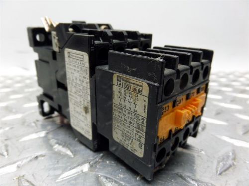
TELEMECANIQUE LC1-D123 A65 & LA1-D31 MOTOR STARTER
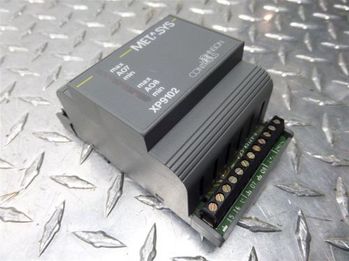
JOHNSON CONTROL METASYS XP9102 XP-9102-8204 9602 UNIT
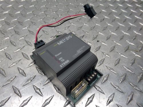
JOHNSON CONTROLS METASYS XT9100 EXTENSION MODULE
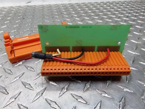
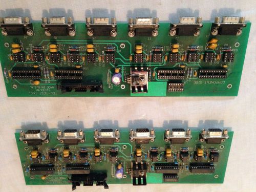
WEIDMULLER RS-NTB3 INPUT BOARD W/ CASE
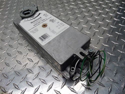
HONEYWELL MS4120F 1006 TWO POSITION DIRECT COUPLED ACTUATOR
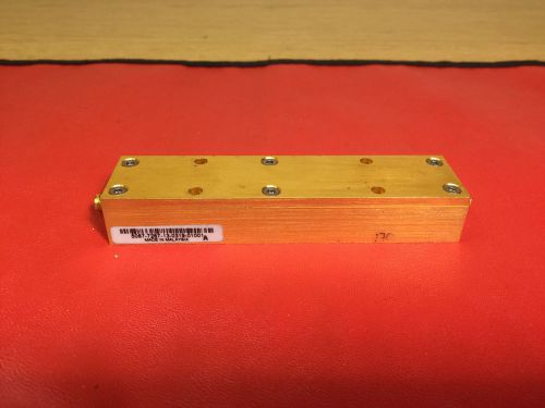
HP Agilent 5087-7267 RF Dual Directional Coupler - Bridge
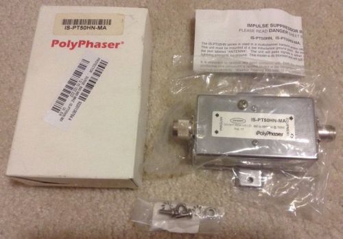
NEW & SEALED! Genuine PolyPhaser IS-PT50HN-MA Coaxial Combiner / Protector #1686
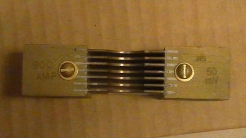
S. E. Co. 900A 50MV 50 Millivolt current shunt SECO 900 AMP RS
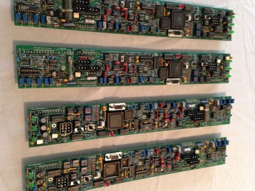
Shunt Heat sink microprocessor control board PT#02024463 REV P1
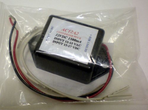
NEW AC12A2 CONVERTER PUCK 12 VDC 1500 MA MAX. ASSEMBLY UNIT
Rs-442 communications isolation component side pt #02024653 rev x1
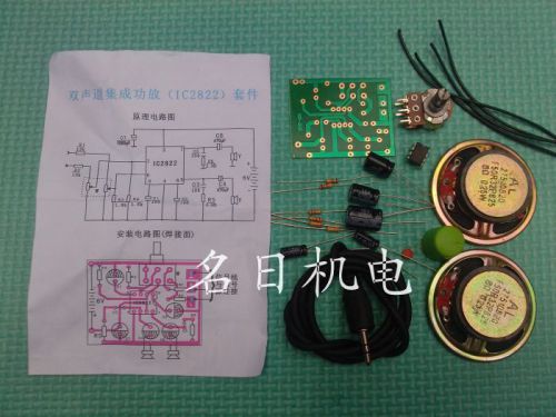
Dual -channel amplifier board/Teaching training components / PCB board DIY kit
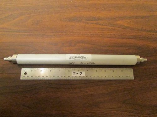
Freedom 503-1024 RF Coaxial Filter BNC Bandpass 56-65MHz
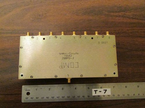
Mini-Circuits ZB8PD-2 SMA Microwave Power Divider 1 to 8
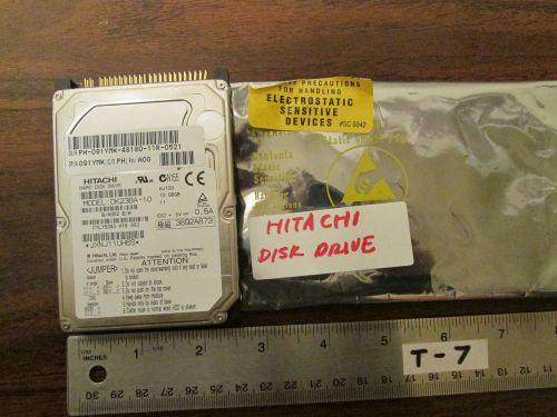
Hitachi Hard Disk Drive DK23BA-10 Laptop Type Small
People who viewed this item also vieved
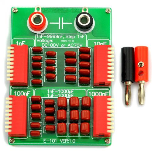
1nF to 9999nF Step-1nF Four Decade Programmable Capacitor Board.
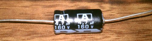
20 pcs 4.7uf 160v Axial Capacitors
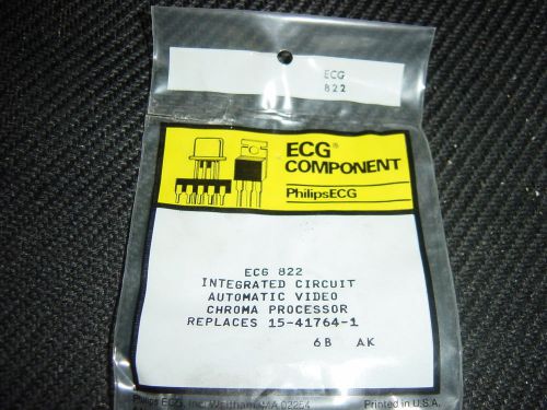
NEW ECG822 INTEGRATED CIRCUIT REPL 15-41764-1, NTE822
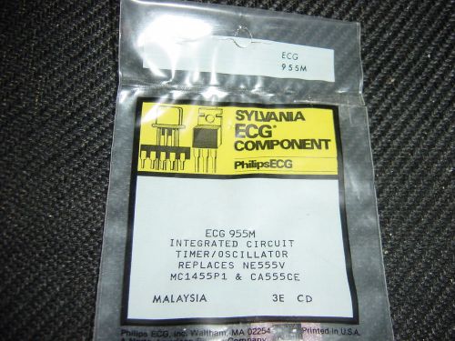
NEW ECG955M INTEGRATED CIRCUIT REPL NE555N, MC1455P, CA555CE, NTE955M
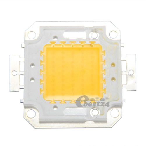
50W Warm White LED IC High Power Outdoor Flood Light Lamp Bulb Beads Chip DIY
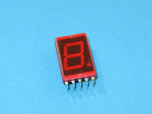
NEC SN713B , 0.45inch 7-segment Red LED Display Common Anode
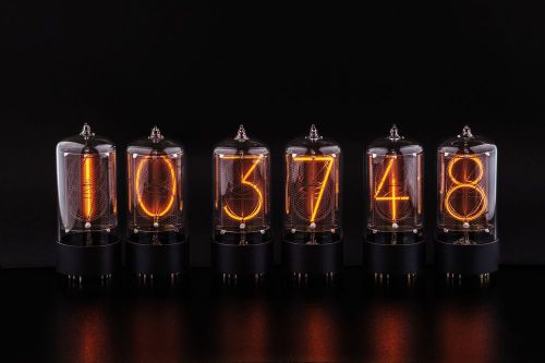
set of 6pcs Handcrafted Nixie Tubes - Large 50mm numbers (2"), Z568M size
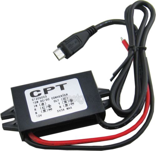
8-22V to 5V DC to DC buck converter power supply MICRO USB Voltage Regulator
Getting Started with Raspberry Pi, 2nd Edition PDF

By clicking "Accept All Cookies", you agree to the storing of cookies on your device to enhance site navigation, analyze site usage, and assist in our marketing efforts.
Accept All Cookies