
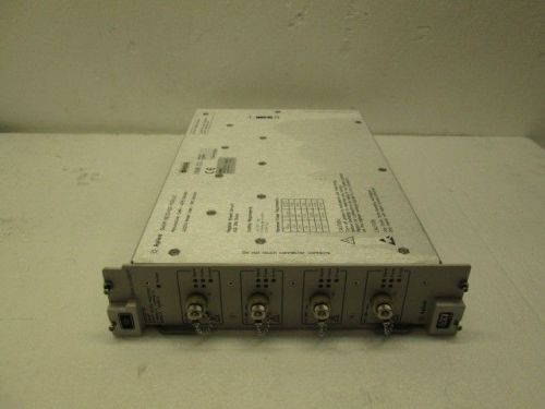
US $299.00
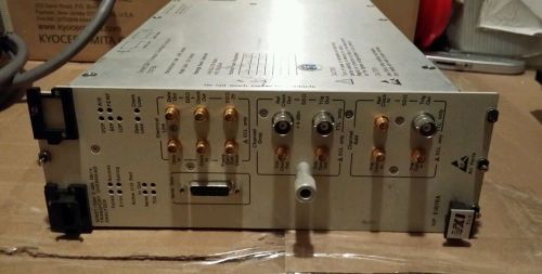
| Condition | Used
:
An item that has been used previously. The item may have some signs of cosmetic wear, but is fully operational and functions as intended. This item may be a floor model or store return that has been used. See the seller’s listing for full details and description of any imperfections.
|
| Seller Notes | “Excellent condition” |
Directions
Similar products from Card Based Modules and Mainframes (VXI/PXI/PCI)
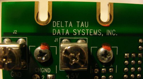
Delta Tau Data Systems Inc. UBUS 6 Sot Back plane 603403-103
AE P/N TCE Body-0.38 Type E S.O 391403.1.1
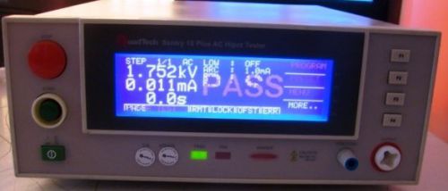
QuadTech Sentry 10 Plus AC Hipot Tester
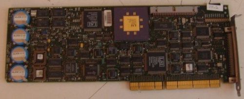
Compaq 003596-001 CONTROLLER2 CHANNEL SCSI
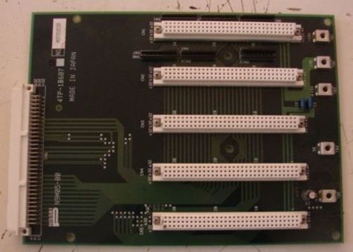
Nisseip 4TP-1B687 No9350539 N9M05-00
038-003-084 Rev A07 TE DGN 0210 UL 380806-001 Board
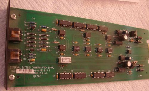
APCC SY CBTMON 640-4118C Rev 4 External Batrey Gear Board
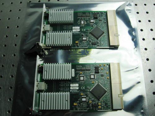
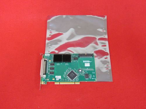
G112419 Lot (2) National Instruments NI-PXI-8330 MXI-3 Boards
MOTOROLA MC1XXX MVME 2604 SBC VME CHASSIS MAIN FRAME SYSTEM W/HUGE LOT OF BOARDS
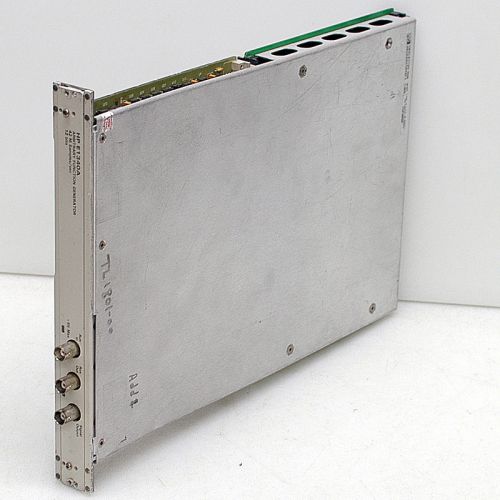
HP E1340A 12-bit 42MSa/S Arbitrary Function Generator VXI Bus with E1340 Adapter
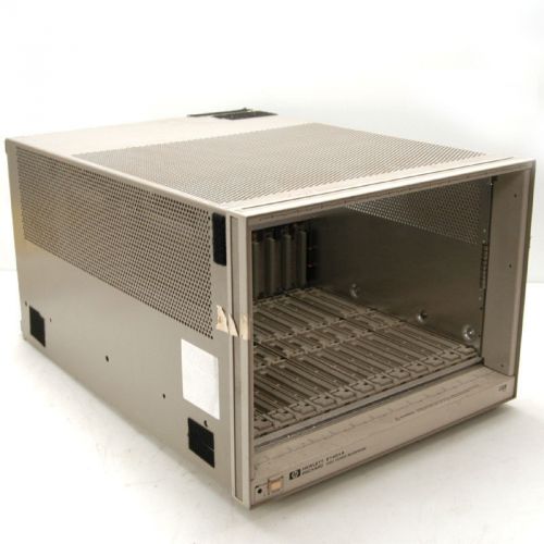
Hewlett Packard HP E1401A Series C VXI Bus Mainframe 13 Slots
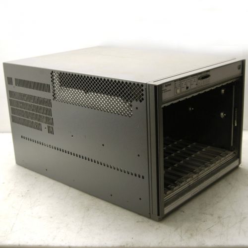
Agilent E8401A C-Size VXI High Power Mainframe 13-Slots
National Instruments NI PCI 6602 DAQ 8-Channel 32 Bit Counter / Timer Board
PCI Bus Extender Logic Analyzer Interface Debug & Validation Board 3V/5V Univ. A
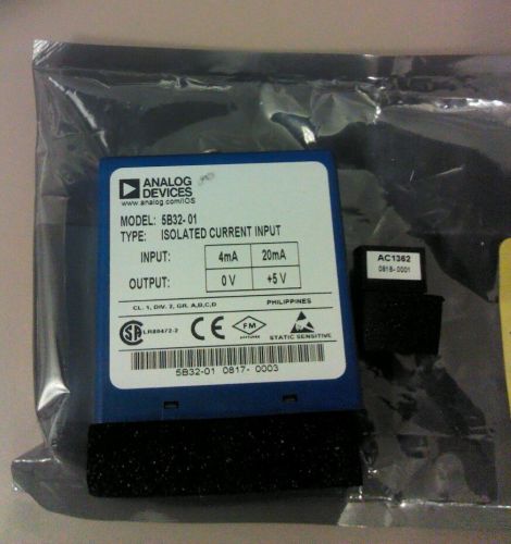
New Analog Devices Isolated Current Input Module 5B32-01
ASC PAD/NI 400 VXI CARD BUS DATA ACQUISITION MODULE 643130-0099 (S8-2-61D)
ACTIS 6U VME CPU BOARD 450MHZ MPC8270 VSBC-6872/FHE-A (S17-T-50D)
HP / AGILENT J4227A DWDM SHORT REACH RECEIVER MODULE
People who viewed this item also vieved
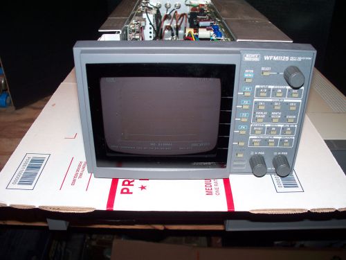
Tektronix WFM1125 HDTV Waveform Monitor
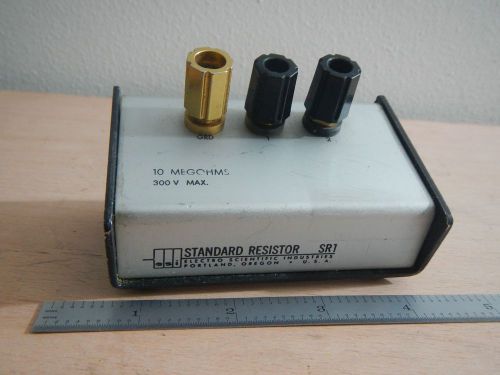
ESI SR1 RESISTANCE STANDARD, 10 MEGOHMS , 300V MAX
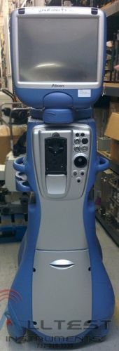
Alcon Laboratories Infiniti Alcon Infiniti Vision System Phaco Phacoemulsifier
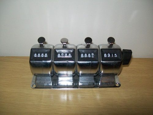
Mechanical Tally Counter, 4 Gang, 4 Digits
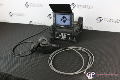
Olympus I-plex MX-R Videoscope Borescope Flaw Detector NDT iPlex Everest VIT
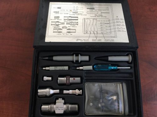
HP 11071A Accessory Kit for 3406 Voltmeter
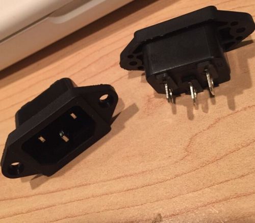
2 PC 3pin IEC 10 A AC Power Cord Inlet Socket Receptacle Panel Mount US Seller!
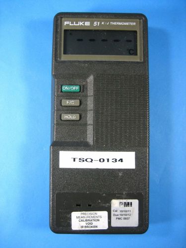
FLUKE 51 K/J - Digital Thermometer
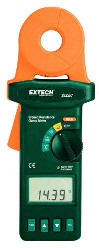
Extech 382357 Ground Resistance Tester
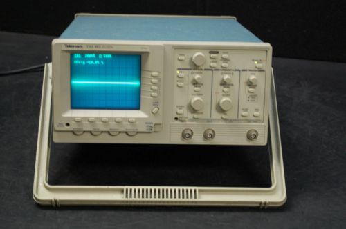
Tektronix TAS465 100MHz 2 ch Oscilloscope
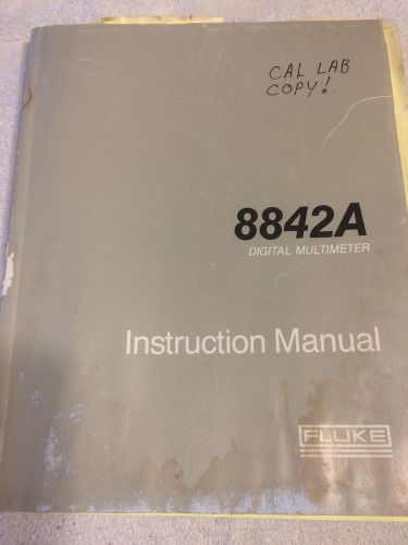
Fluke 8842A Digital Multimeter Instruction Manual (P/N 765313)
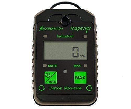
Tough, Waterproof, USA Made: Certified Intrinsically Safe Carbon Monoxide
Power Designs AEC-320-5 Power Supply for NIM Bin Crate
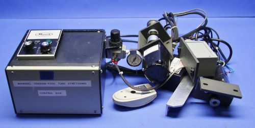
(1) Used Minarik Drives Mandrel Tension Tool Tube Stretching Control Box
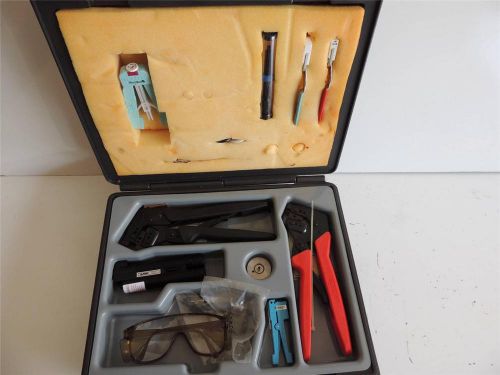
AMP P/N 503330-3 LIGHTCRIMP XTC COMBINED TERMINATION KIT FIBER OPTIC TOOL
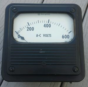
Westinghouse Vintage Antique Amp Meter 500 Amperes AC Steampunk
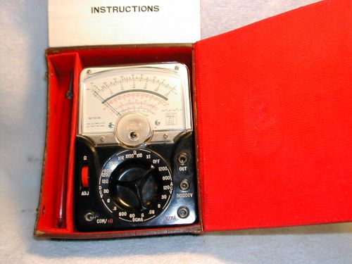
LAFAYETTE 99-50734 MULTITESTER WITH CASE
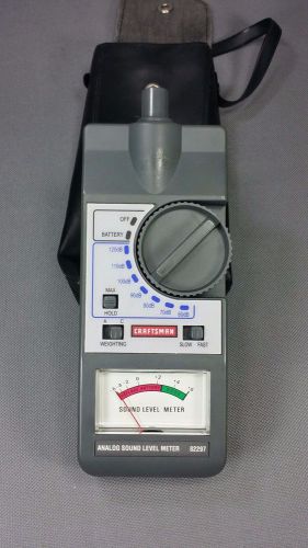
Craftsman Analog Sound Level Meter With Case 60dB - 120dB EUC
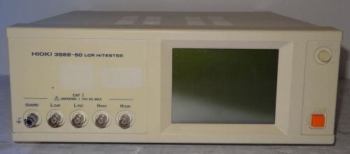
Hioki 3522-50 LCR Meter TESTED!
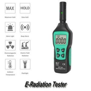
FY876 EMF Meter Dosimeter Detector With the Flashlight Easy to Use No Batteries!
By clicking "Accept All Cookies", you agree to the storing of cookies on your device to enhance site navigation, analyze site usage, and assist in our marketing efforts.
Accept All Cookies