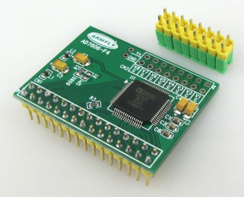
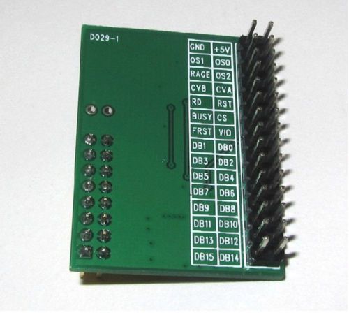
New AD7606 DATA Acquisition Module 16bits ADC 8CH 200Ksps HOME DESCRIPTION PAYMENT SHIPPING TERMS OF SALE ABOUT US DESCRIPTION Tip : To facilitate your choice , PCB board analog input front -row pin (2x8/2.54mm pitch ) default not weld . We will be giving away 2x8 's double needle and eight jumpers from the customer's own choice is up welding, soldering or down . 1, using high-precision 16-bit ADC chip AD7606 2,8 analog inputs. 1M ohm impedance. [No negative supply, there is no front-end analog amplifier can be connected directly to the sensor output] 3, the input range of plus or minus 5V, plus or minus 10V. By IO control. 4, Resolution 16. 5, the maximum sampling frequency sampling rate of 200ksps. Supports eight sampling settings file (which can effectively reduce the jitter) 6, built-in benchmark 7, a single 5V power supply 8, SPI Interface, or 16-bit bus interface. Interface IO level can be 5V or 3.3V. We AD7606 module factory default is 8080 parallel interface. If SPI interface mode, you need to modify R1 R2 resistor configuration. Parallel Mode Jumper: R1 floating (not stickers), R2 10K resistor paste SPI interface mode jumper: R1 stickers 10K resistor, R2 floating (not stickers) AD7606 configuration is very simple, it has no internal registers. Range and over-sampling parameters are controlled via an external IO. Pulse frequency sampling rate provided by the microcontroller or DSP control. AD7606 must use a single 5V supply. Level communication interface between the AD7606 and SCM controlled by VIO pin. That VIO power supply must be connected to the microcontroller can be 3.3V can also be 5V. [Module Pin Description] OS2 OS1 OS2: a combination of state selection oversampling mode. 000 means no oversampling, the maximum sampling rate of 200ksps. 001 represents two times oversampling, which is the hardware inside collected two samples averaging 010 represents four times oversampling, which is the hardware inside collect four samples averaged 011 represents eight times oversampling, which is the hardware inside collected eight samples averaged 100 represents 16 times oversampling, which is the hardware inside collected 16 samples averaged 101 represents 32 times oversampling, which is an internal hardware averaging collected 32 samples 110 represents 64 times oversampling, which is the hardware inside collected 64 samples averaged Oversampling ratio is higher, the longer the ADC conversion time, the lower the maximum sampling frequency can be obtained. CVA, CVB: AD conversion start control signal channel 1-4 decision CVA, CVB decided 5-8 channels. Two signals can stagger a short time, in general, can be CVA, CVB parallel together. RAGE: Select the range of 0 means plus or minus 5V, 1 indicates negative 10V. RD: Read signal RST: Reset signal Busy: Busy Signal CS: chip-select signal FRST: first a channel samples indicating signal VIO: communication interface level DB0 - DB15: Data Bus [16 parallel mode wiring diagram --- AD7606 also supports 8-bit bus mode, see the AD7606 data sheet MCU side AD7606 module GND <----- ground +5 V <----- 5V power supply RAGE <----- can also be connected to the GPIO connected fixed level OS2 <----- can also be connected to the GPIO connected fixed level OS1 <----- can also be connected to the GPIO connected fixed level OS0 <----- can also be connected to the GPIO connected fixed level CVA <----- access the GPIO (output) is used to start AD conversion [Recommended pick pin with PWM output capability] CVB <--- | RD <----- 8080 bus read signal NOE RST <----- GPIO output hardware reset AD606 Busy -----> GPIO input AD606 being converted instructions. [Recommended connection with external pin interrupt capability] CS <----- 8080 bus chip select NCS VIO <----- microcontroller power supply DB0-DB15 -----> 8080 data bus (16) FRST may take [SPI interface mode wiring diagram MCU side AD7606 module GND <----- ground +5 V <----- 5V power supply RAGE <----- any output GPIO, can be accessed by a fixed level OS2 <----- any output GPIO, can be accessed by a fixed level OS1 <----- any output GPIO, can be accessed by a fixed level OS0 <----- any output GPIO, can be accessed by a fixed level CVA <----- access the GPIO (output) is used to start AD conversion [Recommended pick pin with PWM output capability] CVB <--- | RD / SCLK <----- SPI bus clock SCK RST <----- any output GPIO, for hardware reset AD606 Busy -----> GPIO input, AD606 being converted instructions. [Recommended connection with external pin interrupt capability] CS <----- SPI bus chip select SCS VIO <----- microcontroller power supply DB7 (DOUTA) -----> SPI bus data lines MISO DB14 - DB15 may pick FRST may take Software implementations [1] --- timing acquisition of SPI example we offer document using this program, see bsp_spi_ad7606.c In the timer interrupt service routine implementation: Timer interrupt ISR: { Interrupt entry; 8 reads the sampling results are stored in the RAM channel; ----> read is the last record collection for continuous acquisition, it is not related to the Start next ADC acquisition; (flip CVA and CVB) Interrupt return; } Timer frequency is the ADC sampling frequency. This mode can not connect busy port cable. Software implementations [2] --- timed 8080 acquisition of the interface we provide an example of using this program, see bsp_ad7606.c file Configure CVA CVB pin PWM output mode, the sampling period is set to the desired frequency; ---> After the MCU will produce a very stable AD conversion cycle signal The busy port line is set to interrupt falling edge trigger mode; External interrupt ISR { Interrupt entry; 8 reads the sampling results of the channel stored in the RAM; Interrupt return; } [1 and 2, the differences in implementations of software-timed acquisition] (1) Option 1 may be less busy lines, but the other main interrupt service routine or temporary closure of the global interrupt when ADC conversion cycle may cause a slight jitter. (2) Option 2 can ensure the stability of the acquisition of the clock, because it is generated by the MCU hardware, but need more then a BUSY mouth lines. Package includes: 1 x New AD7606 DATA Acquisition Module 16bits ADC 8CH 200Ksps PAYMENT We accept PayPal only. SHIPPING 1.Items are shipped from china.we will send out within 1 bussiness day after receive the payment. 2.We only ship to ebay confirmed address. So before bidding, please kindly verify your ebay address. 3.Shipping to USA takes 8-18 days in normal condition by E-packet with tracking number. Shipping to most other countries takes about 12-30 days via Economy Int'l Airmail. Less than $40, without tracking number,if you request tracking number,please pay $3 more and let me know. Over $40,with tracking number free.The shipping time depends on your location and local postal service,as well as the weather condition along the shipping,sometimes may take longer,.please contact us to confirm before leave feedback or open case. 4.Express shipping: Extra $20 --$25 will be charged for the first 500 grams for most countries. Contact us if you need this service. TERMS OF SALE 1.If you are not satisfied when you receive your item, please return it within 30 days for a replacement or money back. Please contact us before you return it. 2.If item is defective in 30 days, We will send you a replacement without extra charger, or offer refund after we receive the defective item. 3.If item is defective after 30 days, you can still send it back to us. We will send you a new one after receiving the defective item. But you have to pay the extra shipping fee. ABOUT US We are honest seller and do our best to serve you. So if you have any concerns,please don’t hesitate to contact us by ebay message. We will do your best to help you out.please don’t leave negative/ neutral feedback or open case before contact us. On Apr-26-15 at 05:37:42 PDT, seller added the following information:
By clicking "Accept All Cookies", you agree to the storing of cookies on your device to enhance site navigation, analyze site usage, and assist in our marketing efforts.
![[HP] X4000b Bluetooth Wireless Mouse - Matte Black (H3T51AA#ABC) New Unused NIB](/_content/items/images/11/3695211/001.jpg)