US $14.99
| Condition: |
New: A brand-new, unused, unopened, undamaged item in its original packaging (where packaging is
applicable). Packaging should be the same as what is found in a retail store, unless the item is handmade or was packaged by the manufacturer in non-retail packaging, such as an unprinted box or plastic bag. See the seller's listing for full details.
...
|
Country/Region of Manufacture | China |
Directions
Similar products from Other Electronic Monitoring Devices & Assemblies
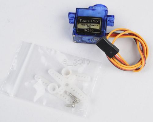
SG90 9G Micro Servo Motor RC Robot Helicopter Airplane controls TowerPro for Arm
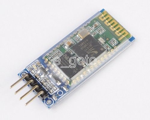
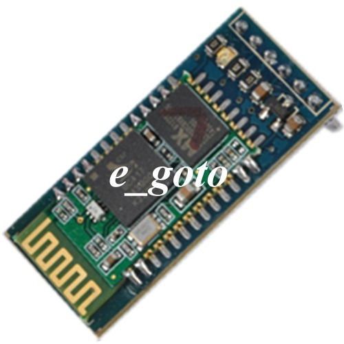
HC-06 Slave Wireless Bluetooth Transeiver RF Module Serial+4p Port line
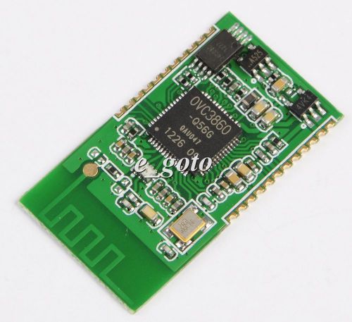
XS3868 Bluetooth Stereo Audio Module OVC3860 Supports A2DP AVRCP Good
RS232/TTL Wireless Transceiver Bluetooth Transceiver Module TTL to RS232 convert
SPK-D Bluetooth Audio Receiver Module MP3 Decoder Card Reader for Arduino
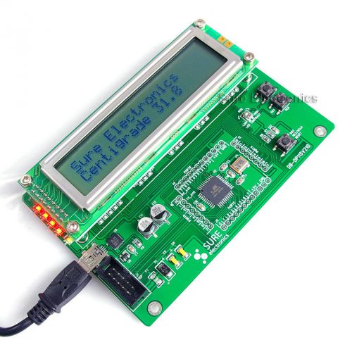
AVR ATMEGA16 Dem2 Demo Development Board LCD & USB
NEW 2.4GHz MRF24J40 Wireless UART Communication Module
SKG16B Bluetooth/RS232/USB UART GPS Module Demo Board
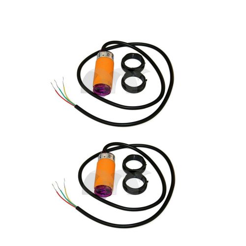
2x E18-D80NK Infrared Obstacle Avoidance Detection IR Sensor
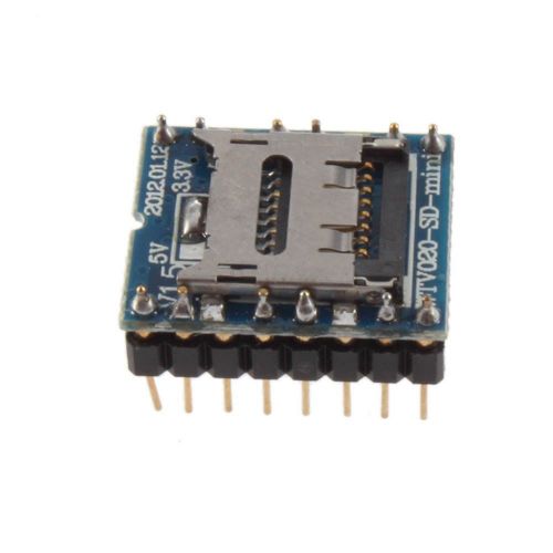
3pcs WTV020-SD-16P U-disk audio player SD card voice/MP3 sound module
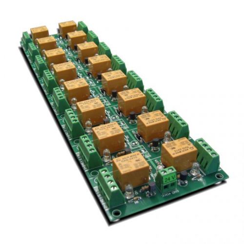
16 Relay Output Module for AVR, PIC Project, 24V

Encoder wheel meter wheel length measuring wheel circumference 204mm
Incremental photoelectric rotary encoder ZSP3806-3600P/R 3600 pulse ABZ
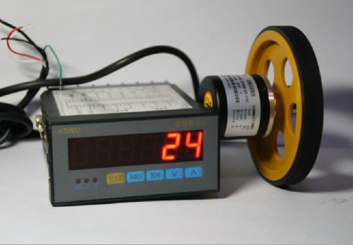
Positive inversion counter meter + 400P/R encoder + meter counting wheel set
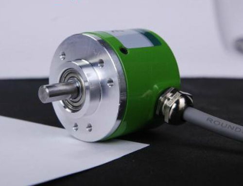
High precision pulsed Straight carved photoelectric 3600P/R rotary encoder
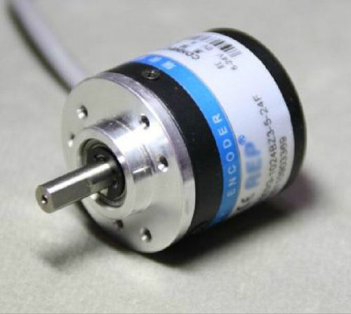
Incremental photoelectric rotary encoder 400P/R AB phase 5-24V
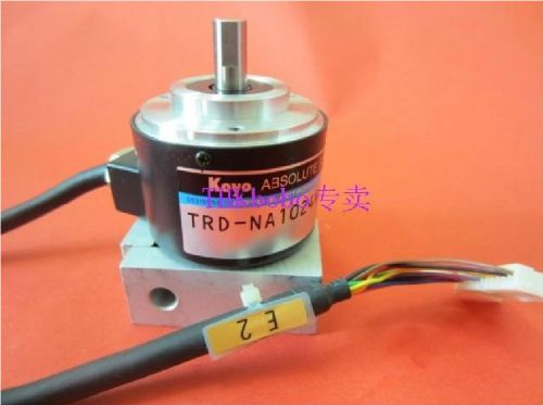
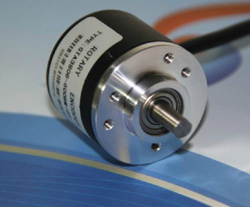
1024P/R Koyo encoder TRD-NA1024NW
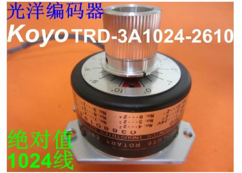
Original Koyo Encoder TRD-3A1024-2610 1024P/R
OMRON E6B2-CWZ1X 720P/R ROTARY ENCODER
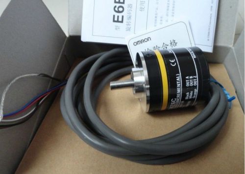
New OMRON Rotary Encoder E6C2-CWZ6C 1500P/R
People who viewed this item also vieved
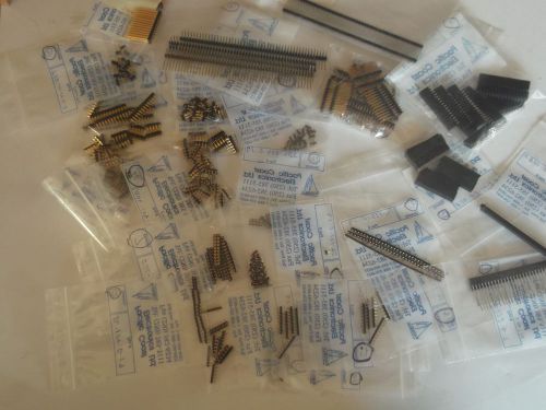
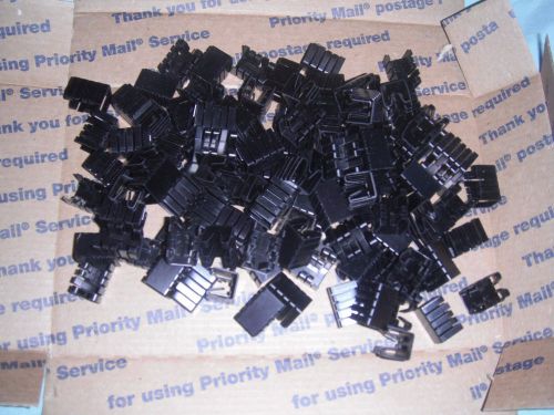
LARGE SELECTION OF PCB HEADERS & SOCKETS NEW SAMTEC, M/L, ETC AS PICTURED
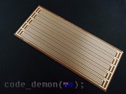
Prototype PCB 8.5 x 20cm Universal Matrix Printed Circuit Board - Arduino / AVR
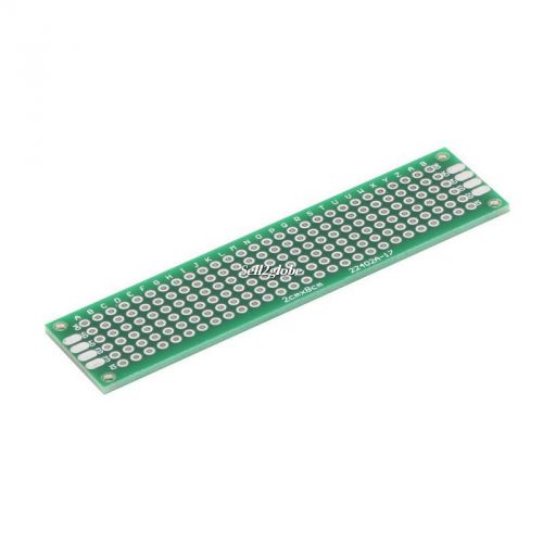
Double Side Prototype PCB Tinned Universal Breadboard 2x8cm 20mmx80mm New G8
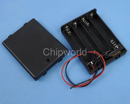
1PCS 4XAAA 4xAAA 6V Battery Holder Box Case Wire Omniseal with Shield AAA
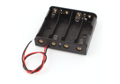
Generic Lead Black Storage Case Box Holder with Wires for 4 x 1.5V AA Batteries
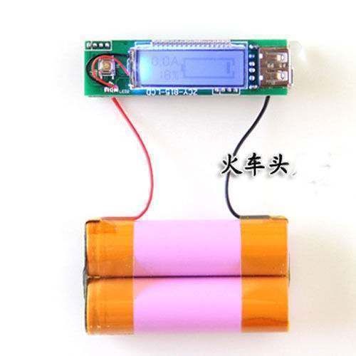
Lithium ion 2.1A 3.7V TO 5V USB Boost Charge Board LCD Mobile power
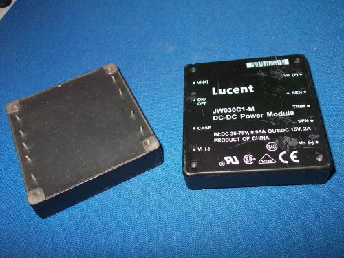
JW030C1-M LUCENT DC-DC Conv 30W LUCENT JW030C1 TRIMMED LEADS
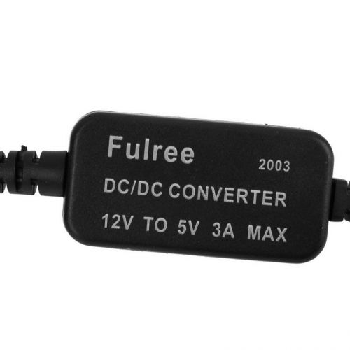
DC 12V to 5V 3A Step down Converter Regulator to 2 Female USB Output for Car &
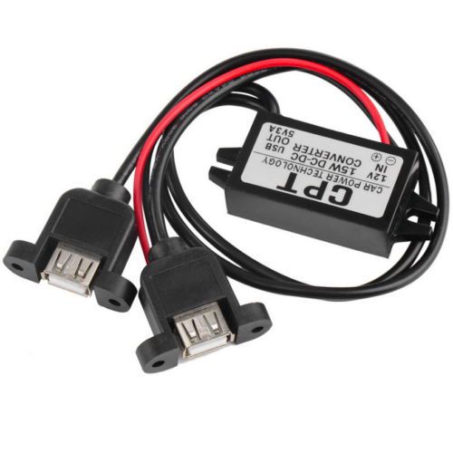
DC DC Converter Module 12V To 5V 3A 15W Duble USB Output Power Adapter &
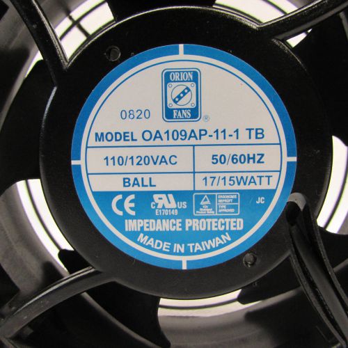
Orion Fans OA109AP-11-1 TB 110/120VAC 50/60Hz 17/15W Metal Box Fan
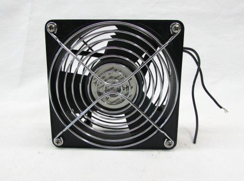
Hoffman A-4AXFN 115VAC 85-100 CFM Metallic Box Fan
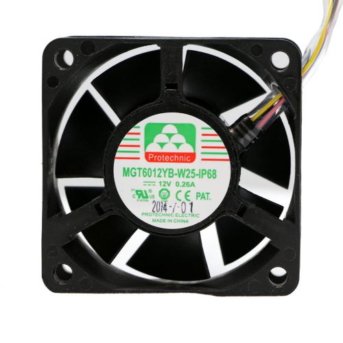
Protechnic 60mm IP68 Waterproof Fan MGT6012YB-W25 IP68 12VDC 27.28 CFM
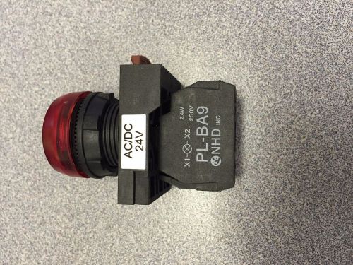
NHD NPL22-RA (Red) Pilot Lamp Round Head 24V
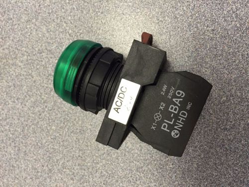
NHD NPL22-GA (Green) Pilot Lamp Round Head 24V
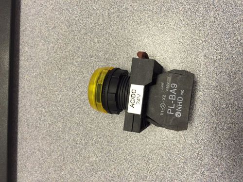
NHD NPL22-YA (Yellow) Pilot Lamp Round Head 24V
Heat sinks. TO-220 clip on style.
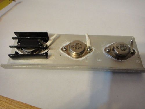
3 Transistor Heatsink with two 2N3055 and one MJ4033 TO-3 type IC's
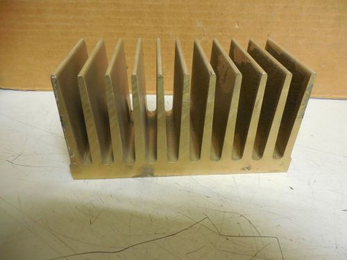
NO NAME ALUMINUM HEAT SINK SYNC 6" INCH x 3" INCH x 3" INCH
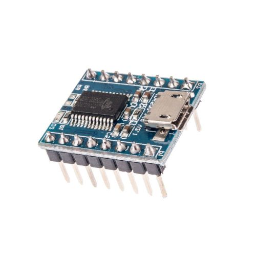
1PCS New JQ6500 Voice Sound Module USB Replace One to 5 Way MP3 Voice Standard
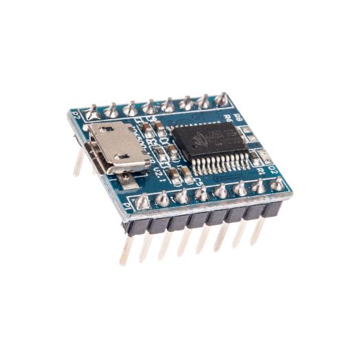
JQ6500 Voice Sound Module USB Replace One to 5 Way MP3 Voice Standard New
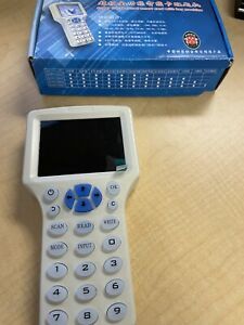
RFID Copier Cloner Card 10 Frequency
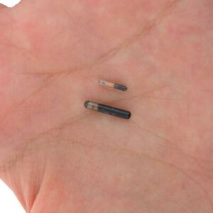
134.2KHZ Microchip Animal RFID tag for Fish dog cat idetification QM
Impinj Speedway Revolution RFID Reader IPJ-REV-R420-USA1M w/A6001 Hub A6051 GPIO
By clicking "Accept All Cookies", you agree to the storing of cookies on your device to enhance site navigation, analyze site usage, and assist in our marketing efforts.
Accept All Cookies