US $340
Directions
Similar products from Other Electronic Components & Spare Parts
CP2102 USB 2.0 to TTL UART Module 6Pin Serial Converter STC Replace FT232 Module
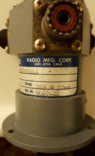
Jennings RC41E6000N44 High Powered Coaxial Coax Vacuum Relay WORKS
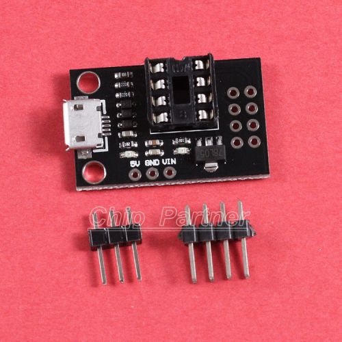
Development Programmer Board Micro USB for ATtiny13A/ATtiny25/ATtiny45/ATtiny85
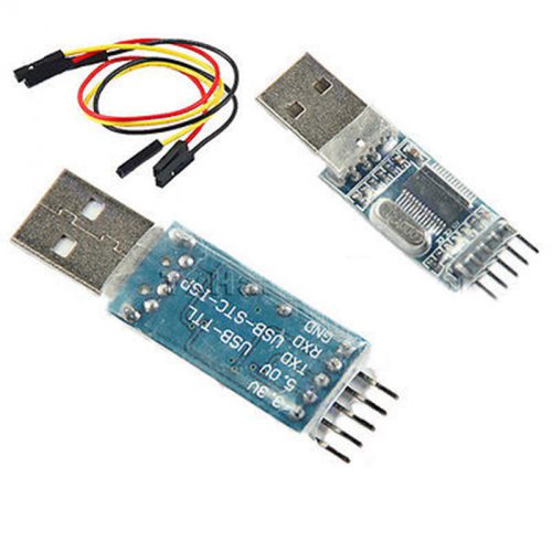
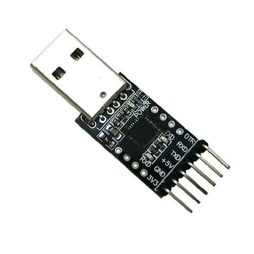
USB To RS232 TTL PL2303HX Auto Converter Module Converter Adapter For arduino
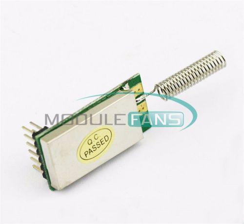
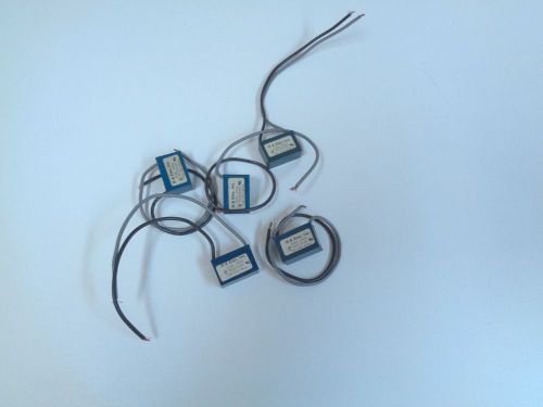
SI4463 Wireless Transceiver Module With Spring Antenna 2000M GOOD Quality
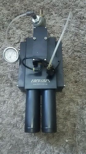
EDCO USA DML200N-ES Quad Vacuum -ES 12/05 gauges, fittings VSA18-NOP USED,

2X ESP8266 Remote Serial Port WIFI Transceiver Wireless ESP-12E+antenna -NodeMCU
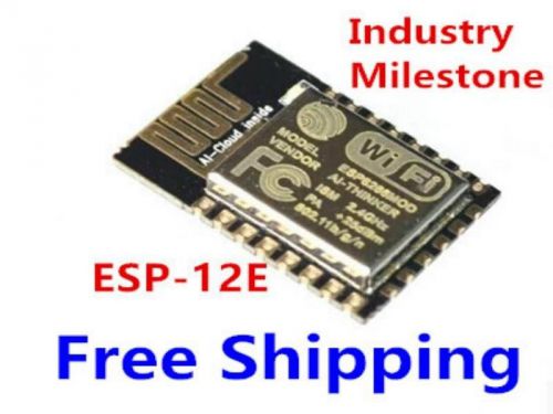
5X ESP8266 Remote Serial Port WIFI Transceiver Wireless ESP-12E+antenna -NodeMCU

10X ESP8266 Remote Serial Port WIFI Transceiver Wireless ESP-12E+antenna-NodeMCU
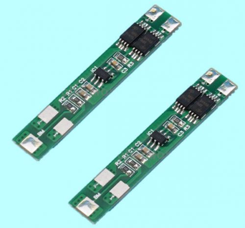
2PCS 7.2V 6A 2S Dual MOS Polymer Lithium Battery Protection Board for 18650
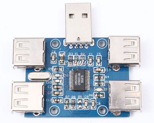
5V USBHUB USB2.0 Hub Concentrator 4-Female Precise USB Expansion Module
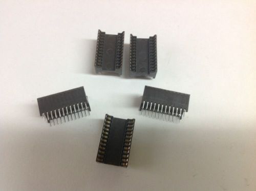
Lot of Five: 24 Pin IC Socket Pin Through Hole Solder DIP High Profile Wide Type
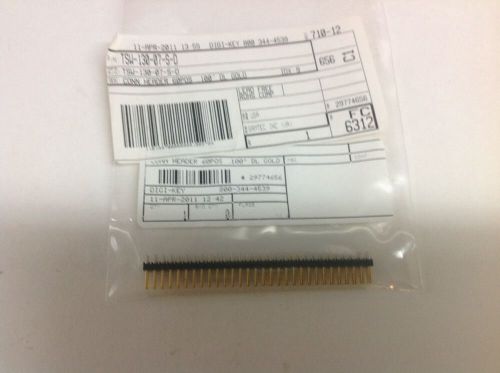
New Samtec 60 position .100 Gold Header Pin Board to Board Connector Solder PCB
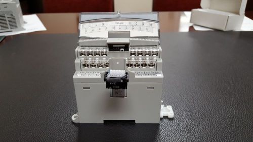
Allen Bradley MicroLogix Digital input module, 1762-IQ16
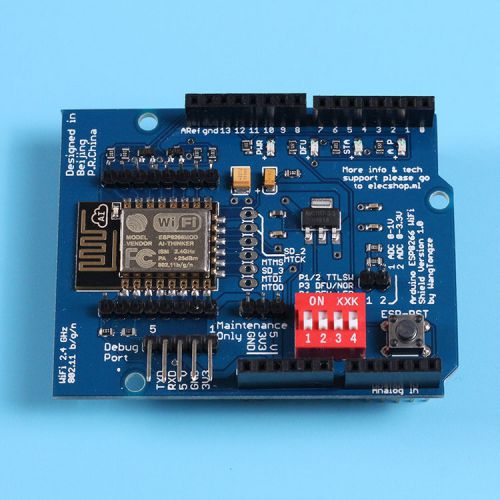
ESP8266 ESP-12E UART WIFI Wireless Shield for Arduino UNO R3
Electronic Components Lot of 10 - Capacitors, resistors, rectifier,counters
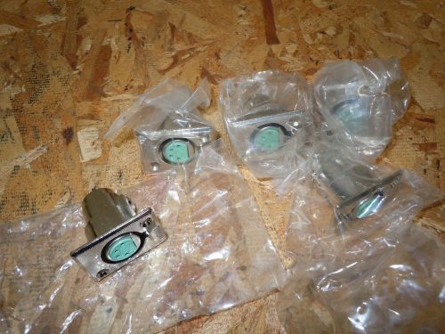
Switchcraft , D4F Front Loading Panel Mount 4 Pin XLR Connectors 4 PIN Lot of 5
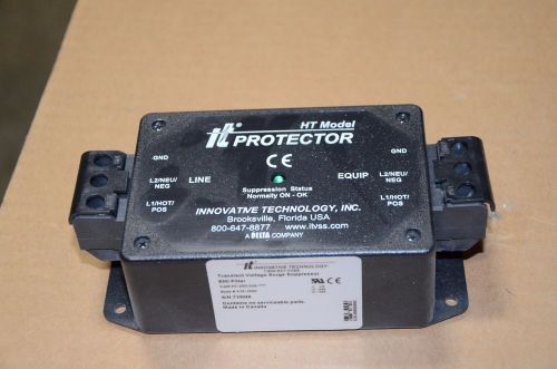
Innovative Transient Voltage Surge Suppressor EMI Filter HT-250-30A 415-1600 HT
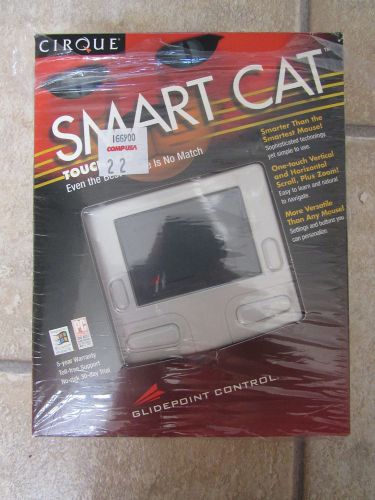
CIRQUE GDB410 SMART CAT GLIDEPOINT CONTROL SERIAL & PS/2 INTERFACE
People who viewed this item also vieved
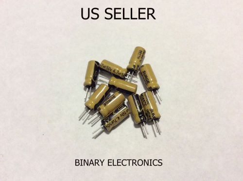
20pcs Nichicon 4.7uF 50v Low Leakage Radial Electrolytic Capacitor USA SELLER
R-K ELECTRONICS RCS7A-6V SNUBBER SUPPRESSOR - LOT OF 5 BRAND NEW! FREE SHIPPING
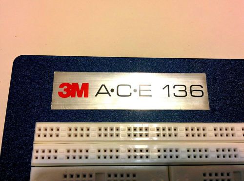
3M ACE-136 Solderless BreadBoard,3048 tie points, NEW, Digikey Part#923339-I
![[1x] Yellow 170 Point Solderless PCB Mini Breadboard - Ships FAST from USA!](/_content/items/images/28/1983028/001.jpg)
[1x] Yellow 170 Point Solderless PCB Mini Breadboard - Ships FAST from USA!
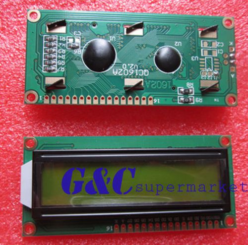
2PCS 1602 16x2 HD44780 Character LCD Display Module LCM Yellow backlight
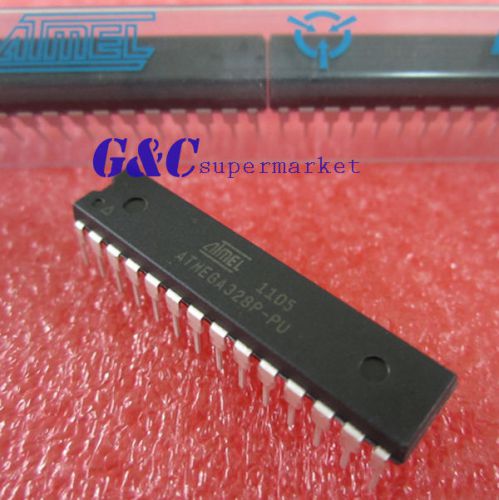
5PCS ATMEGA328P-PU DIP-20 Microcontroller NEW DATE CODE:12+
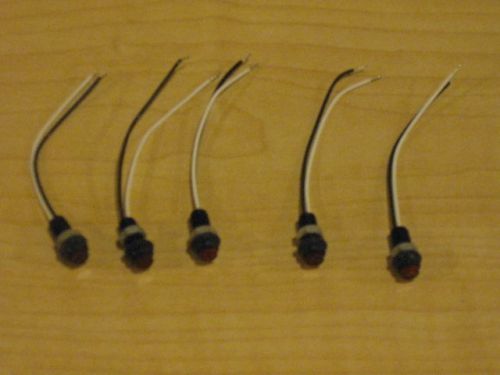
LEDs for Electronics Projects - 5 Pieces - Red - With Mounting Nut
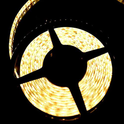
Wholesales 10PCS 5M 3528 300 LED SMD Warm White LED Strip Light IP65 Waterproof
1xE88CC Telefunken made in Germany Amplitrex AT1000 Tested #1108001
1pair ECC83 Brimar made in U.K. Amplitrex AT1000 Tested #1100001&1103001
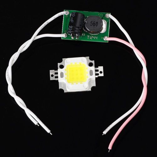
High Power 10W 9-12V DC White LED Light Bulb 900-1000LM + DC12V-24V Driver
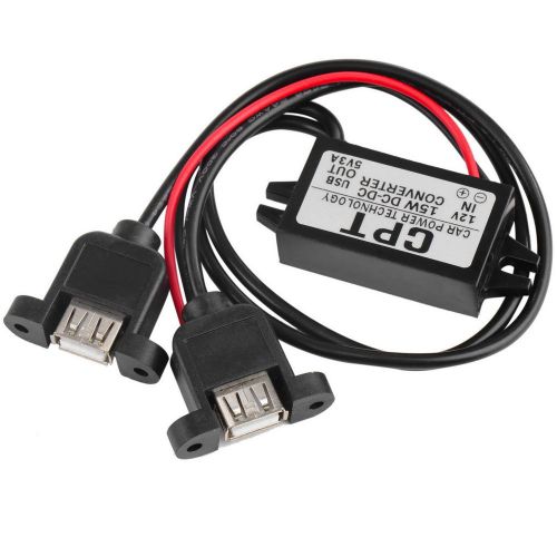
DC DC Converter Module 12V To 5V 3A 15W Duble USB Output Power Adapter EC
Make: Getting Started with Sensors PDF

By clicking "Accept All Cookies", you agree to the storing of cookies on your device to enhance site navigation, analyze site usage, and assist in our marketing efforts.
Accept All Cookies