US $3300
Directions
Similar products from Other Equipment for Electrical Testing
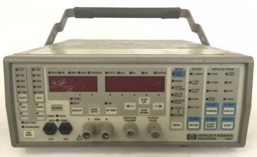
HP 4934A Transmission Impairment Measurement Set TIMS
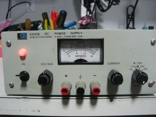
HP AGILENT 6200B DC POWER SUPPLY 0-40V, .75A/ 0-20V, 1.5A
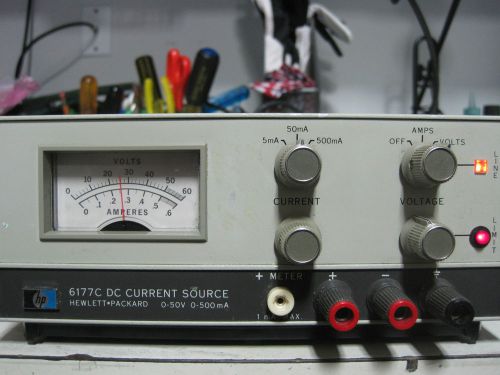
HP AGILENT 6177C DC CURRENT SOURCE 0-50V 0-500mA
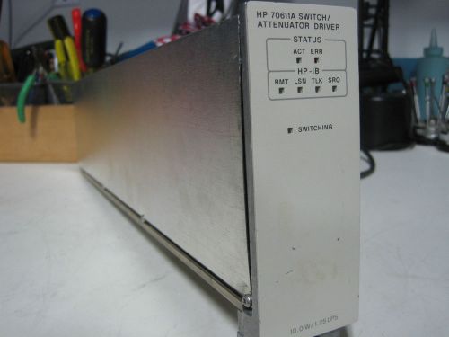
HP AGILENT 70611A SWITCH/ATTENUATOR DRIVER
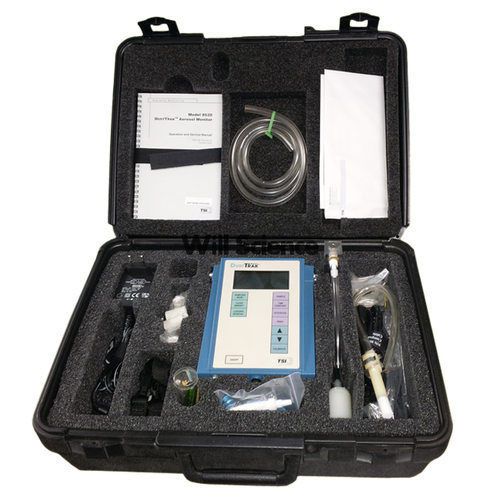
TSI DustTrak 8520 Aerosol Monitor in case with all Accessories!
HP 4934A Transmission Impairment Measurement Set TIMS w/ Case
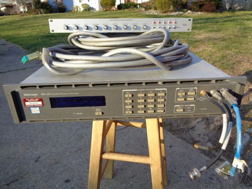
Lot of 2 Tektronix TDC-10 Tunable Down Converter and 3240 Processing Amplifier
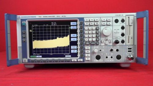
Rohde & Schwarz FSQ40 /B25,B72,K70 Spectrum Analyzer, 20 Hz to 40 GHz
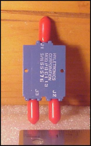
2-Way RF SMA Power Divider / Combiner - 10 Mhz to 10 Ghz
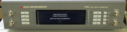
EG&G/PAR/Signal Recovery 7265 DSP Lock-In Amplifier .001Hz-250KHz *NEW*CAL!
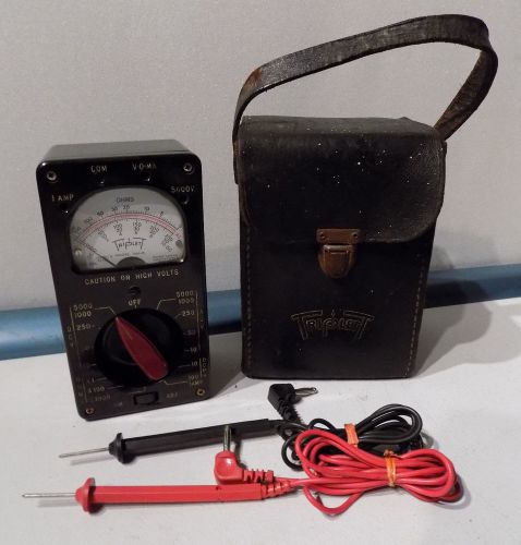
VINTAGE RARE TRIPLETT MODEL 666-R OHMS ELECTRICAL MULTI METER W/CASE BAKELITE NR
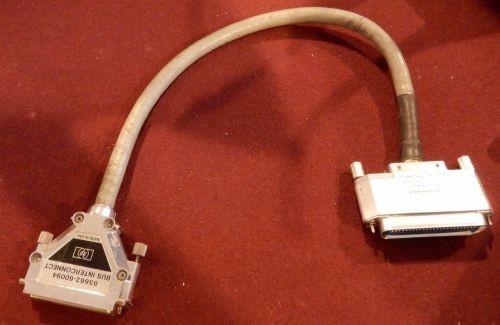
HEWLETT PACKARD HP MODEL 85662-60094 BUS INTERCONNECT CABLE
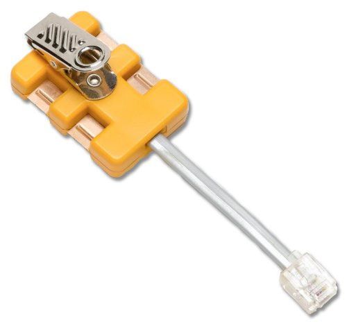
Fluke Networks 10113000 4-Wire Modular Adapter
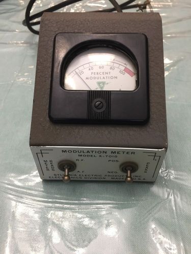
Sylvania Electric Modulation Meter Type X-7018 - Rare Find . Working Nice!!!
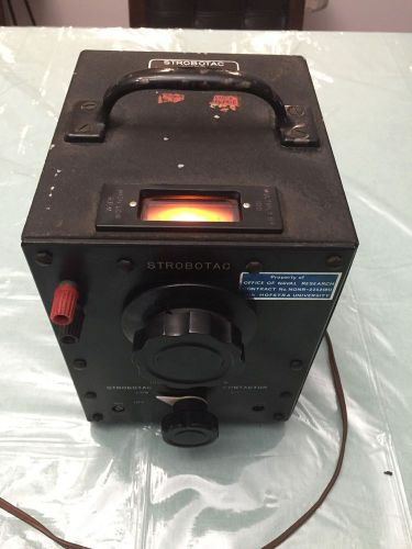
Vintage General Radio 631-B Strobe Light Strobotac Nice And Working !!!!!!!!!!!!
Ithaco 4213 Electronic High/Low/Band Pass Filter Preamplifier Preamp w/ Opt 02
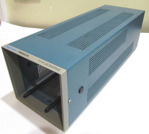
TEKTRONIX TM502A Power Module 2 Slot for TM500 series plug-ins
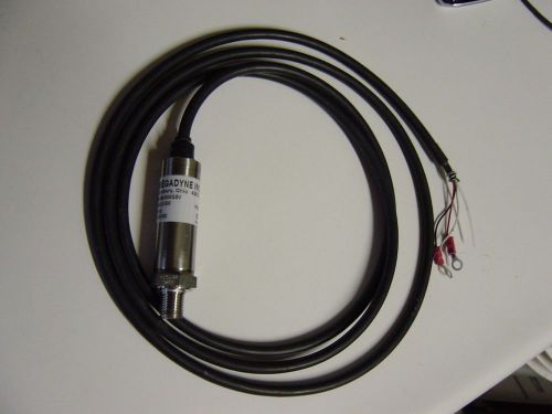
Pressure Transducer Omegadyne Inc PX409-500G5V 0-500
People who viewed this item also vieved
Agilent E7008A Calibration Unit
Agilent/Keysight 5350B 10Hz to 20GHz CW Microwave Counter, Opt 010
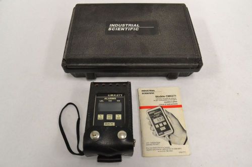
INDUSTRIAL SCIENTIFIC CMX271 MULTI GAS MONITOR DETECTOR B294173
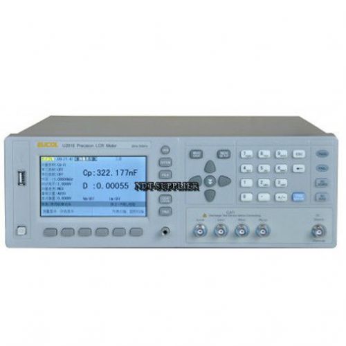
New U2817 Precision LCR Meter Tester 50Hz – 100kHz, 16 Points, 0.1V, 0.3V, 1.0V
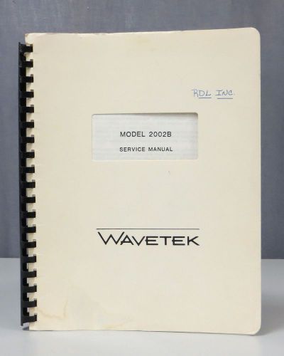
Wavetek Model 2002B Sweep/Signal Generator Service Manual
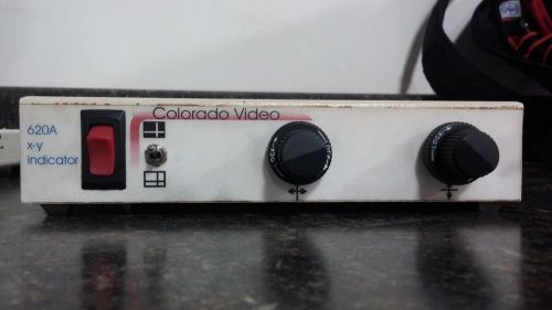
Colorado video 620A X-Y indicator
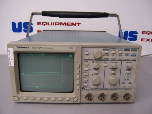
8413 TEKTRONIX TDS 420 4 CHANNEL OSCILLOSCOPE 150 MHZ 100MS/s
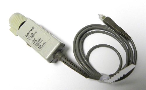
TEKTRONIX PROBE 10X 1.5 GHZ MODEL P6245
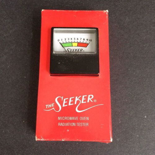
Vintage "The Seeker" Microwave Oven Tester RADIATION
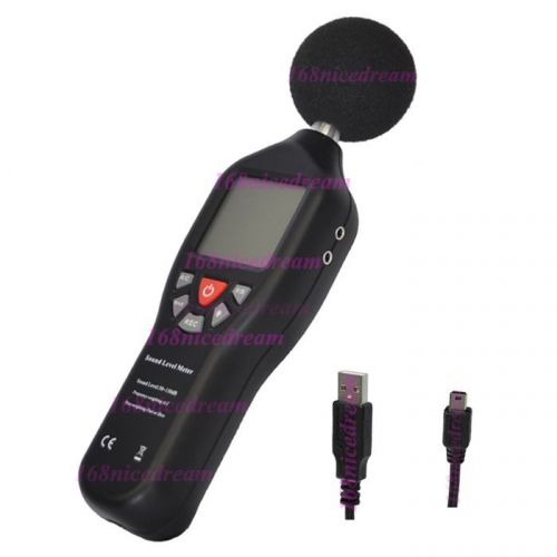
Digital USB Sound Meter Noise Level 30 ~ 130dB 31.5Hz~8kHz Record 32K Data N0300
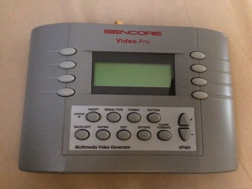
Sencore VP401 VideoPro Multimedia Video Generator ONLY Power Port Needs Repair
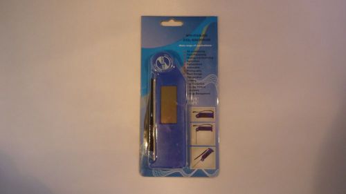
Digital Thermometer Temperature Meter Gauge with Folding Sensor Pointed Probe
Computerized Cardmatic Tube Tester Upgrade for *Your* Hickok or Western Electric
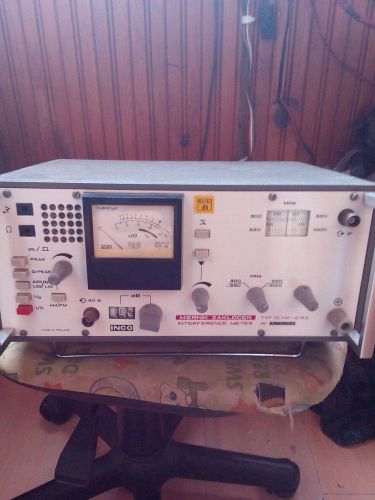
Interference meter DLMZ-4/50 ,AM/FM
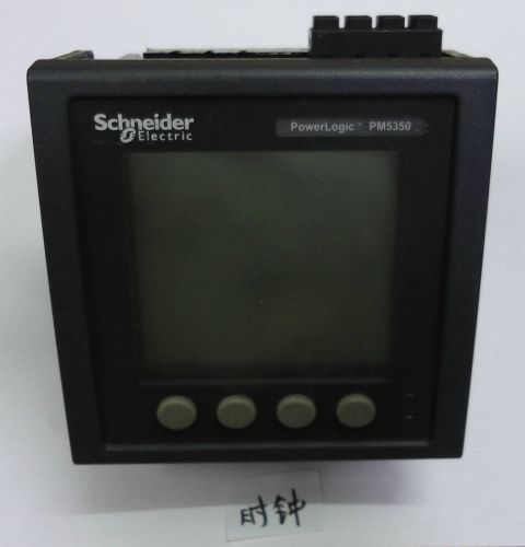
Schneider Eiectric Power Logic PM5350
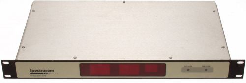
Spectracom 8183 Netclock GPS Satellite Atomic Clock Receiver 1PPS IRIG Timecode
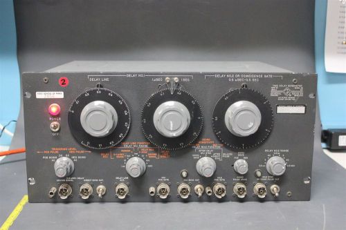
VINTAGE GENERAL RADIO TIME DELAY GENERATOR 1392-A
By clicking "Accept All Cookies", you agree to the storing of cookies on your device to enhance site navigation, analyze site usage, and assist in our marketing efforts.
Accept All Cookies