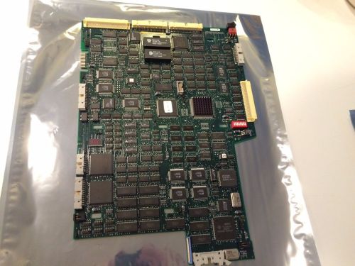
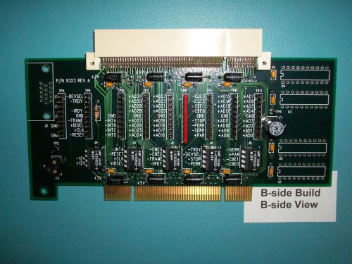
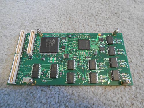
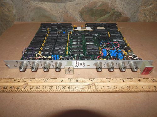
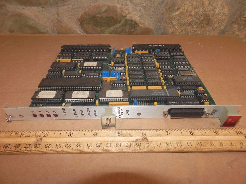
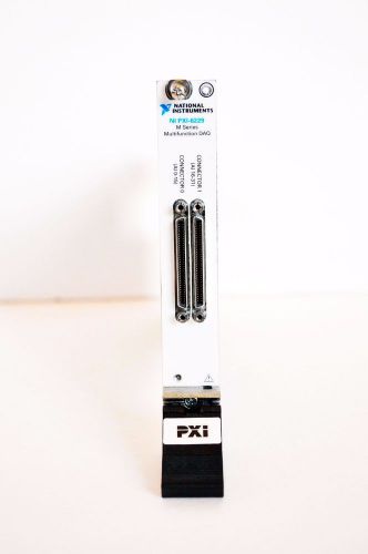
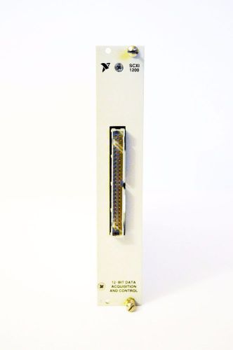
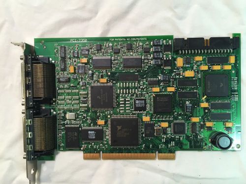
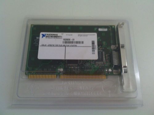
This board is a multi-purpose passive Universal 3.3-volt / 5-volt, 32-bit Conventional PCI 2.0 through 2.3 card designed to interface a motherboard to test equipment (such as logic analyzers, oscilloscopes, and current meters) for debugging, product validation, test and measurement, and reverse engineering. It can be used by itself as a cost-effective PCI interface or extender ("riser") card, or accept a Device Under Test in the upper slot, supporting the isolation of the most common PCI signals from the motherboard with disconnect switches supporting new peripheral design development. This listing is for an B-side component build. It is also available reversed, as a A-side build in a different listing. Be sure to select the correct build for your needs. The B-side component bulid provides isolation switches and test points mounted on the surface of the board that faces you when the backplate (mounting bracket) is on your left, and the key notch is on your right. A detailed Product Information Page and downloadable Product Manual contain additional details on the product features and usage and are available online for your convenience. Customers will receive schematics, layouts, and a recommended logic analyzer wiring configuration with their purchase. This is a professional product, validated through years of use in industry, and I guarantee it will meet your needs or you may return it in undamaged condition within 14 days for a full refund. Note: This is a legacy device: Conventional PCI version 2.2 and 2.3: 3.3V/5-volt universal card, for performing analysis in systems that are Conventional PCI (not PCI-Express, which is a serial bus, not parallel like this device). It accepts universal (mixed 5V/3.3V) cards in the upper slot and does supply 3.3V to the upper connector when the fuse F2 (not included) is installed. It is keyed as a universal card on the bottom (male end) only. It typically fits into a white connector, but if you're reading this, you already know that. Please be aware that the upper connector is keyed 5V only, so if you put this interface card into a really old 5V motherboard and put a 3.3V card in the upper slot, you hypothetically could damage your device under test if it was poorly designed. You will not damage your device under test if it fits into the motherboard directly, and you install the 3.3V fuse (not included but available on request) on this card and then use it in the top slot. Summary of Product Features * High-quality 4-layer board with power and ground planes on inner layers, plus electrolytic and tantalum decoupling capacitors to reduce noise and ground bounce. Best quality parts including very reliable Burndy connector and AMP DIP switches. * All PCI signals are routed through the card, with most bus control signals able to be disconnected with the installed individual signal isolation switches. Most (but not all) bus signals are routed to header pins. Some unused header pins are provided for user customization. * Signals are clearly labeled on the silkscreen on both sides of the board. * Reversible build - purchase your preferred stuffing option with components installed on the A-side or the B-side so that test points are oriented "outward" regardless of physical constraints of motherboard component orientation or arrangement of other installed peripheral cards or riser cards. * Not specific to a particular logic analyzer. The user can probe any desired subset of signals by connecting the header pins to any analyzer's "flying leads" or an oscilloscope probe. * Weak (10K) pullups are provided for the PCI control signals FRAME#, STOP#, IRDY#, TRDY#, DEVSEL#, RESET#, and CLK, so that they are deasserted on the extender card's top receptacle if the signals are disconnected from the bus with the switches. The peripheral under test can be hard reset by opening the switch and grounding its RESET# input (accessible at the RESET# switch). * Test pin dimension and spacing accommodate all standard logic analyzer probes: standard 0.1 inch spacing, 0.025 inch square test pins. * Plenty of ground points are provided for grounding logic analyzer pods and scope probes. * Four 20-pin sockets connected to +5V (pin 20) and GND (pin 10) are provided for prototyping such as with 16V8 GALs or other programmable logic such as to support "Using Delayed FRAME# to Differentiate Address Phases." * Fuses are installable and removable on the 3V and 5V supply rails for isolation testing, current consumption measurements, and to help prevent accidental shorts from causing board or component damage. Power plane test points are provided for easy access to drive the peripheral under test with external power supplies (with the fuse removed). * Weak (10K) pulldown is provided on the IDSEL signal so it is deasserted when disconnected with the isolation switch. * Components on the board are not sensitive to ESD. (Optional DFRAME# modification excepted). * Manufactured in U.S.A. A Note About Component Builds This board is a reversible design. Inspect your system configuration to determine which side of the board you want the isolation switches and test points mounted in relation to the backplate (card bracket) and key, especially if you are working with a system using a riser card or limited space between boards. Here is a useful image showing PCI Keying. For more information, refer to the Conventional PCI pinout specification on Wikipedia, or the actual PCI specification. The Wikipedia article visually demonstrates the differences between the 5V and 3.3V keyings, and the pinout is clearly and conveniently referenced looking down into the motherboard connector. Please verify that you are ordering the component build orientation that meets your needs. Shipping charges, Fuse F2, the mounting bracket, and the VGA connector for attaching the mounting bracket are not included. For an additional $50, I will modify your board to generate a delayed FRAME# output which can be used to differentiate Address from Data phases in PCI transactions. State listings can then be set up to exclude all wait states, or further qualified to store only particular transaction types. This is excellent for timing software operations or hardware events, for determining burst lengths or merge behavior, and for comparing performance of time-critical software implementations for device drivers for PCI devices. This product is not the only option for performing PCI bus analysis. This comparison chart from the Product Information Page provides some detail about the specific differences between this 9323A board and some competing products. Powered by eBay Turbo Lister The free listing tool. List your items fast and easy and manage your active items.
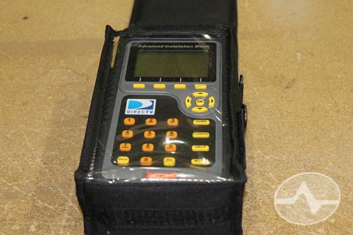
By clicking "Accept All Cookies", you agree to the storing of cookies on your device to enhance site navigation, analyze site usage, and assist in our marketing efforts.
![[National Instruments] NI PXI-8105 Dual-Core 1GB Ram NI PXI 1031 PXI Base TESTD](/_content/items/images/72/5821872/001.jpg)
![[National Instruments] NI PXIe-8106 Dual-Core 1GB Ram TESTED + 80GB Hard disk](/_content/items/images/69/5821869/001.jpg)