US $1,000.00
Directions
Similar products from Card Based Modules and Mainframes (VXI/PXI/PCI)
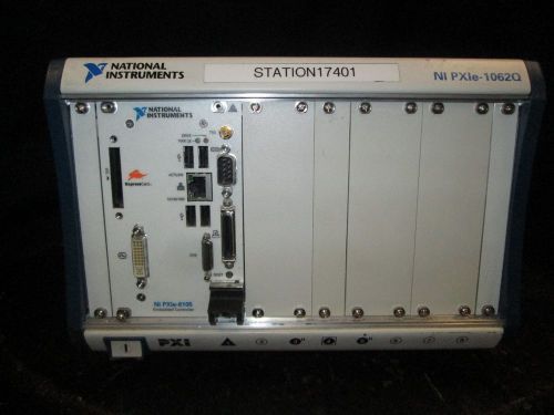
National Instruments NI PXIe-1062Q w/NI PXIe-8105 XP Pro COA
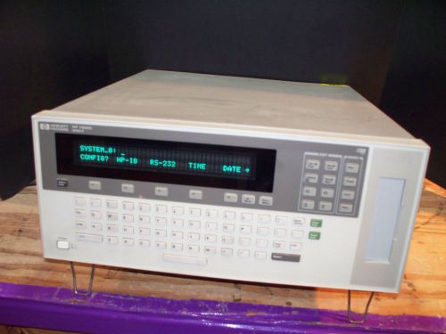
HP 75000 Series B Measurement System Mainframe
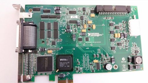
National Instruments PCIe 6323
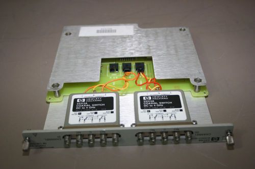
Keysight Agilent 44476B Microwave switch & Qty 2 33313A Coaxial Switch, DC-4Ghz
*Tested* National Instruments NI PCI-6229, 32 Channel 16-Bit, M-Series DAQ
*Tested* National Instruments NI PCI-6602 8-Channel 32-Bit Counter/Timer Module- show original title
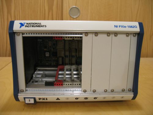
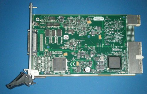
National Instruments NI PXIe-1062Q / 8-Slot 3U Express Chassis Up to 3 GB/s
Dawn VME Products VMEbus Extender Board XB400ADT1
Electronic Solutions VME bus Extender Board VME-68ED C1023 (qty 2)
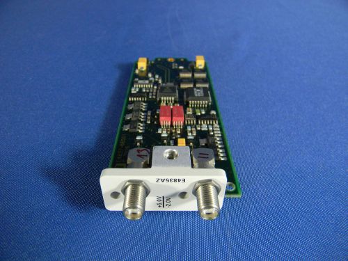
Agilent E4835AZ ParBERT 675Mb/s Differential Analyzer Front-end 30 Day Warranty
National Instruments NI PCI DIO 96 Interface Card 182920E 01
National Instruments NI PCI DIO 32HS Parallel Digital I/O Interface Card 183480D
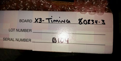
Innovative Integration X3-Timing precision timing card PCIe GPS
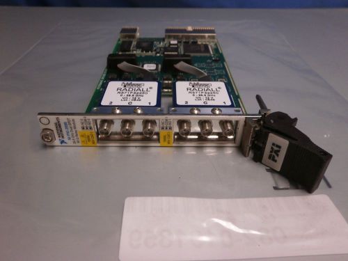
National Instruments NI PXI-2599
![[National Instruments] 186736C-01 PCMCIA-GPIB card only EMS / UPS Fast Shipping](/_content/items/images/55/4145055/001.jpg)
[National Instruments] 186736C-01 PCMCIA-GPIB card only EMS / UPS Fast Shipping
*Tested* National Instruments NI PXI-6220, 16 Channel 16-Bit, M-Series DAQ
Used Good MATRIX MFG 8216A Function Generator, No cable #ES3
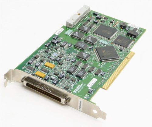
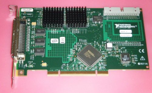
NATIONAL INSTRUMENTS NI PCI-6024E DAQ 16-CH 12-BIT MULTIFUNCTION BOARD CARD- show original title
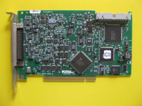
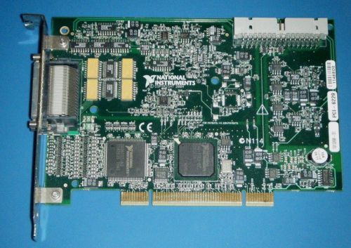
NATIONAL INSTRUMENTS PCI-MIO-16E-4 MULTIFUNCTION DAQ CARD- show original title
Matrox Pulsar 586-04 Rev B Image Processing PCB Board,PNS5307,MY10910,used,Canad
People who viewed this item also vieved
Varian Triscroll 300 PTS03001 uvpi Scroll Pump
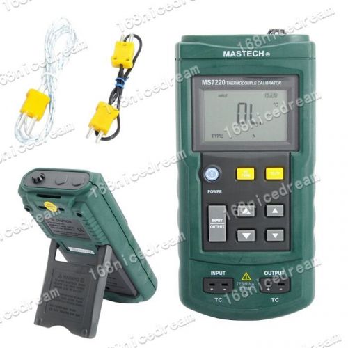
MASTECH MS7220 Thermocouple Simulate/Calibrator TC/mV Output Tester Meter N0159
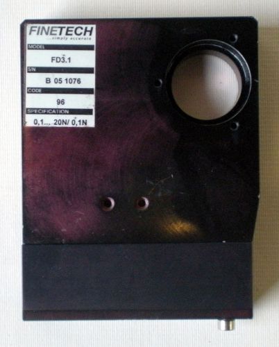
FINE-TECH MODEL FD3.1 CODE 96 SPEC: 0,1...20N/0,1N OPTICAL MOUNT STAGE ASSEMBLY
Electro-Technic Products no. 4001 dc variable voltage electrical testing tool
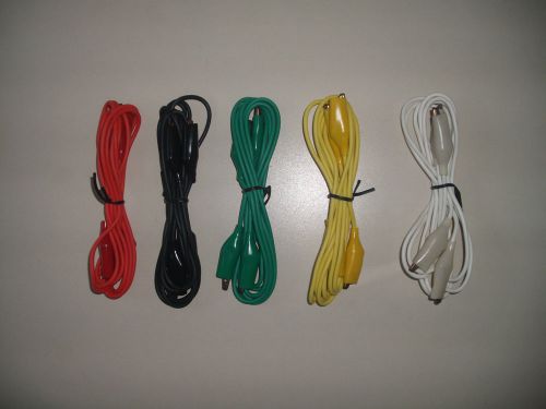
20 PIECE TEST LEADS ALLIGATOR ROACH CLIP JUMPER WIRE 32"
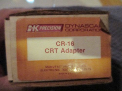
BK B&K Precision CR-16 SOCKET ADAPTERS 470 480 490 CRT TESTER "NOS" B&K
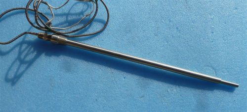
23 3/4 “ Stainless Steel Temperature probe & well
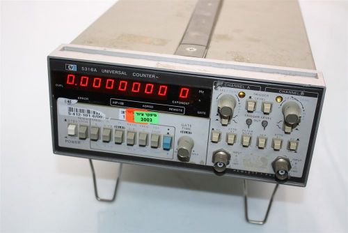
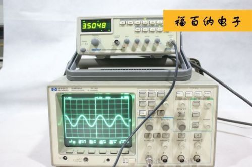
HP Agilent Hewlett Packard 5316A 100 MHz Universal Counter
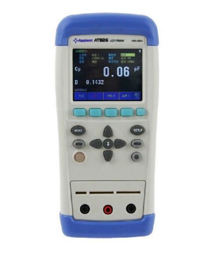
New AT826 handheld LCR Digital Bridge
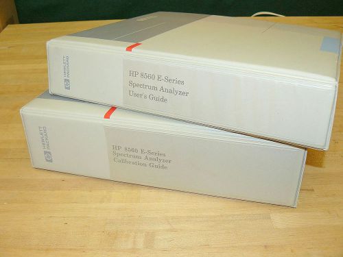
HP HEWLETT-PACKARD 8560 SPECTRUM ANALYZER USERS GUIDE CALIBRATION GUIDE MANUALS!
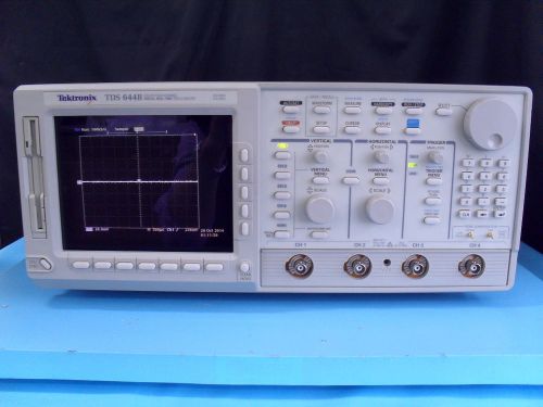
Tektronix TDS644B w/P6139A x 2 Digital Oscilloscope
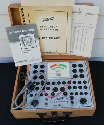
Vtg 1959 Century Fast Check Tube Tester FC- 2 Original Owner Complete Working
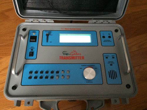
Berkeley Varitronics Gator Transmitter 20 Watt Class A
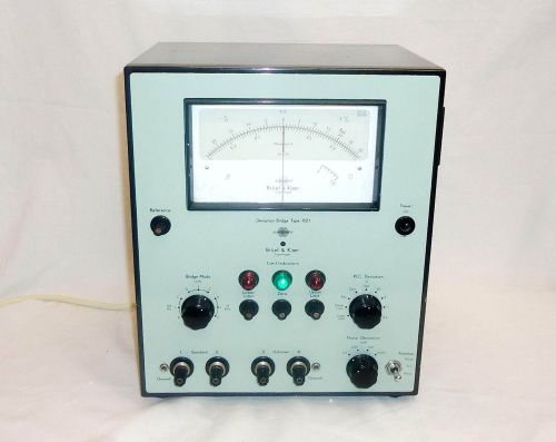
Bruel & Kjaer Deviation Bridge Type 1521
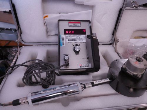
Victoreen 660 660-1 gamma radiation and x-ray dose measuring rate detector
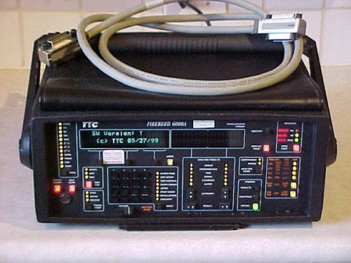
TTC Fireberd 6000A Communications Analyzer Options 6001, 6002, 6003, 6005, 6009
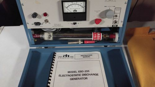
Andy HISH ESD 255 Electrostatic Discharge Generator W/ Probe & Original Manual
Leader Model LVS-5850B NTSC Vectorscope
By clicking "Accept All Cookies", you agree to the storing of cookies on your device to enhance site navigation, analyze site usage, and assist in our marketing efforts.
Accept All Cookies