US $3.00
Directions
Similar products from Analog Semiconductors, Amplifiers & Modules
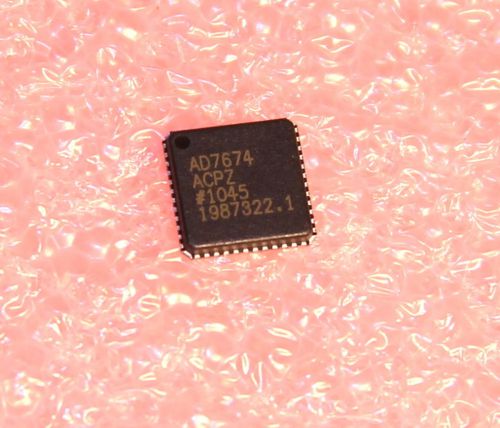
AD7674 ADC 18-Bit, 2.5 LSB INL, 800 kSPS SAR AD7674ACPZ Analog Devices: -:
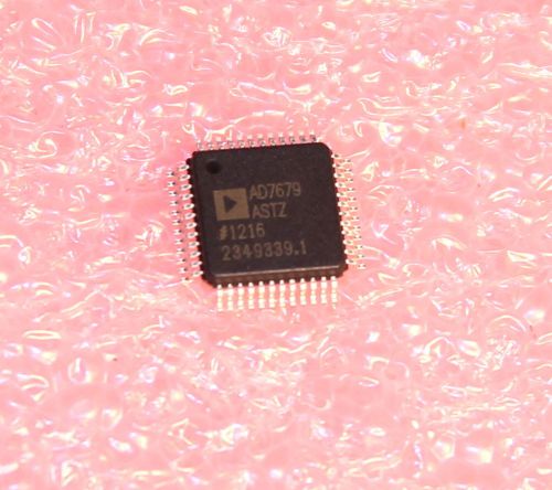
AD7679 ADC 18-Bit, 570 kSPS PulSAR A/D Converter AD7679ASTZ Analog Devices: -:
AD7690 ADC Differential 18-Bit, 1.5 LSB INL, 400 kSPS AD7690BRMZ : -:
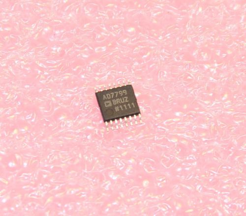
AD7799 ADC 3-Channel, Low Noise, 24-Bit, Sigma Delta w IN-amp AD7799BRUZ: -:
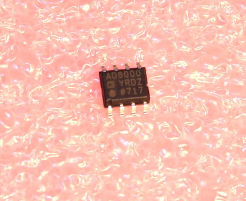
AD8000 1.5 GHz Ultra-High Speed OpAmp w Power-Down AD8000YRDZ Analog Devices:
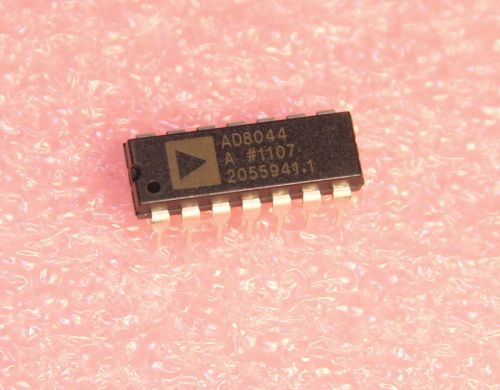
AD8044ANZ Quad 150 MHz Rail-to-Rail Amplifier OpAmp AD8044ANZ Analog Devices: -:
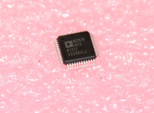
AD7676 ADC 16-Bit, 2.5 LSB INL, 500 kSPS SAR AD7676ASTZ Analog Devices: -:
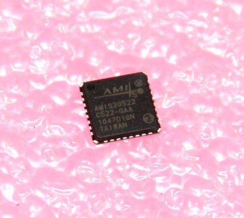
AMIS30522 Bipolar Stepper Motor Driver Micro-Stepping SPI interface free ship
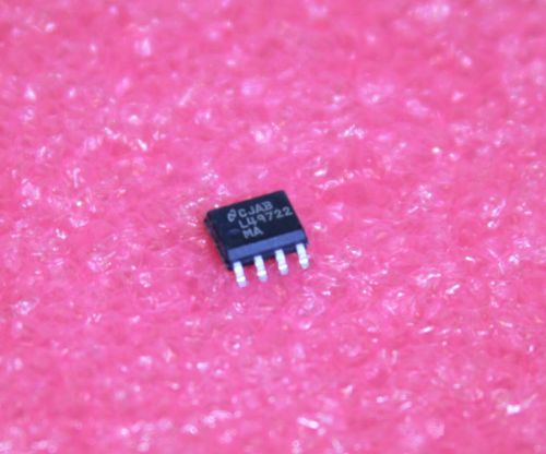
LME49722 Dual ultra low noise low THD Audio Opamp LME49722MA -:
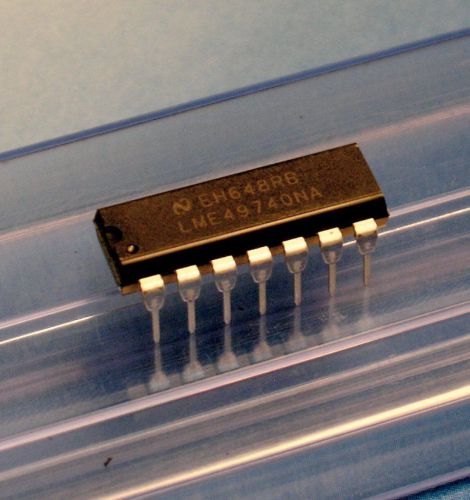
LME49740 Pro Audio Quad Low Noise OpAmp PSRR 120 DIP-14 -:
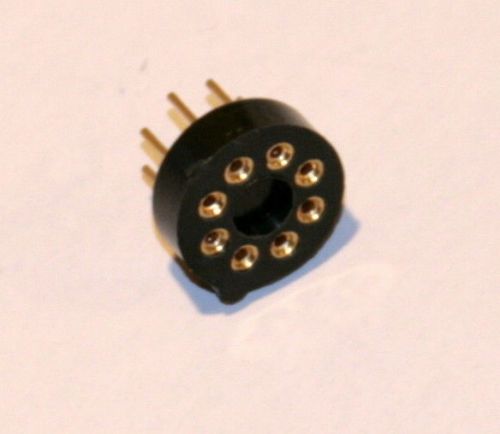
Machine pin socket for TO99 case ICs Hi-Rel gold inlay -:
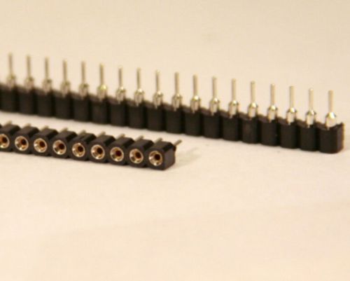
Machined Pin Header, Female 40 pos. precision machine socket (x2 -:
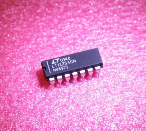
LT1125 Quad Low Noise, High Speed Precision Op Amp LT1125ACN ltc -:
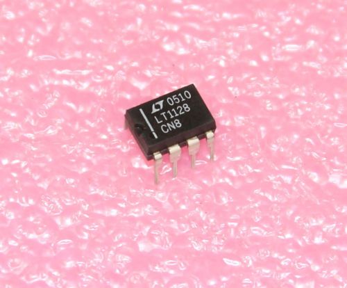
LT1128 CN Ultralow Noise Precision High Speed Op Amp LT1128CN ltc -:
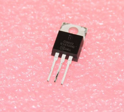
MBR16100 MBR16100CT SCHOTTKY Diode Rectifier 100V 16A Qty:4 -:
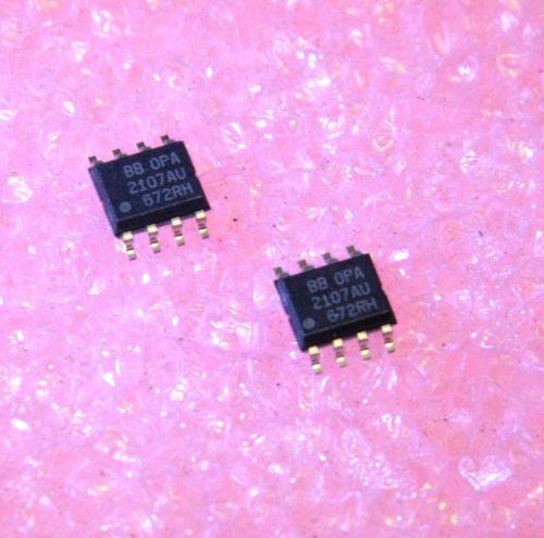
OPA2107 dual Low Noise Difet OpAmp Pro audio SOIC8 (4) -:
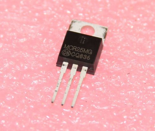
MCR25 SCR Thyristor 25A 600V MCR25MG Qty:2 -:
![MC33152 [x2] MOSFET IGBT driver Dual 1.5A 15ns non-inverting MC33152P -:](/_content/items/images/61/2012261/001.jpg)
MC33152 [x2] MOSFET IGBT driver Dual 1.5A 15ns non-inverting MC33152P -:
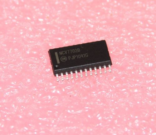
NCV7702 1 A Dual H-Bridge Motor Driver Automotive Rated NCV7702B -:
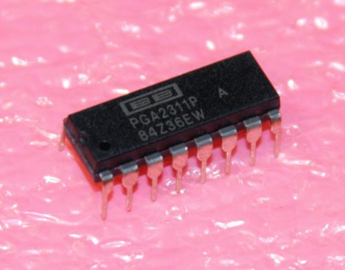
PGA2311 Digital Stereo Audio Volume Control, Low Noise, USA parts PGA2311PA -:
People who viewed this item also vieved
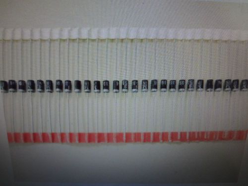
500 Pieces of 1N5391 Diodes, Manufacturer MSC
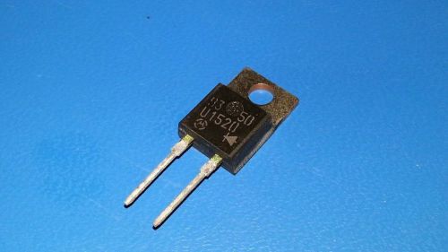
5 pieces, U1520 Ultra Fast Rectifier Diode, NOS
500 Pieces of 1N4738A Diodes, Manufacturer Transitron
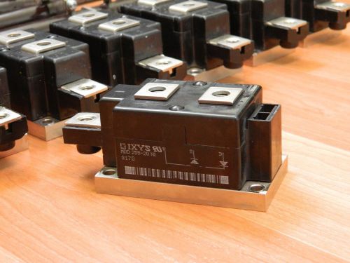
High Voltage High Power Diode Module - 2,000 Volts 450 Amps - IXYS MDD 255-20N1
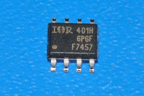
35-PCS FET/MOSFET N-CHANNEL 20V 15A IR IRF7457 7457
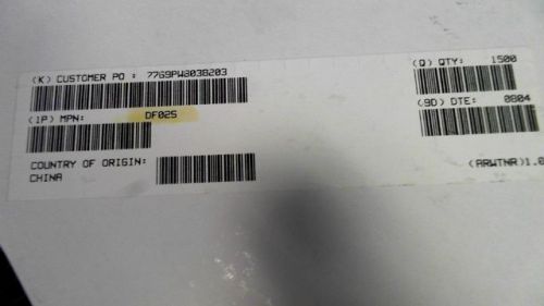
400-PCS BRIDGE 200V 1.5A FAIRCHILD DF02S DF02
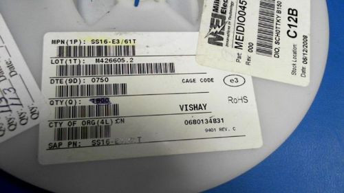
113-PCS SCHOTTKY 60V 1A VISHAY SS16-E3/61T 16E361 SS16E3
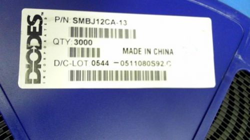
605-PCS BI-DIRECTIONAL 12V 600W DIODES SMBJ12CA-13 12CA13 SMBJ12CA13
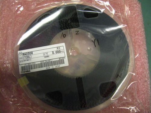
3000PCS TOSHIBA RN2308 (TE85L) Bipolar Transistors 100mA -50v 3Pin 22K x 47Kohm
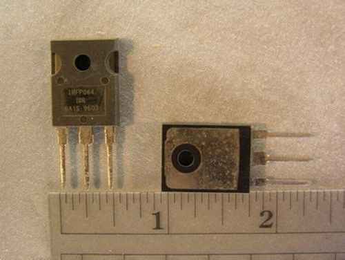
5 International Rectifier IRP064 N-Channel 60V 70A HEXFET Power MOSFETs
Box of 800 DIODES Inc Low Dropout Regulator P/N AP1117KL-13
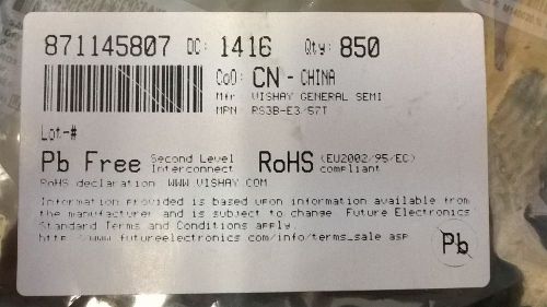
VISHAY RS3B-E3/57T Diodes Lot of 850 DIODE GEN PURP 100V 3A DO214AB
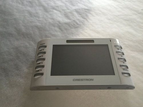
Crestron Wall Mount Touch Panel/TPMC-4SM
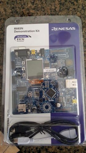
Renesas Synergy Demonstration Kit RX63N
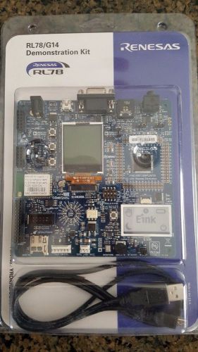
Renesas Synergy Demonstration Kit RL78/G14
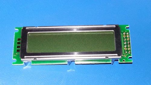
1 Piece, Seiko LCD Display Module L1672 Dml D01 003 94V-0, NOS
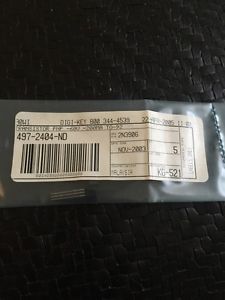
2N3906 -60V -200MA TO-92 Transistors in sealed package of 5
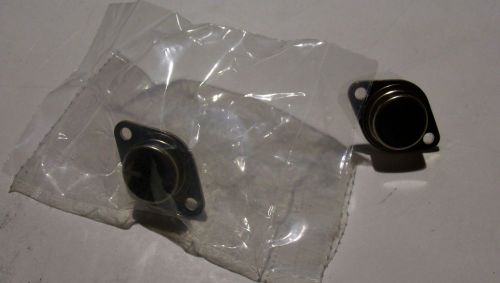
Two Motorola TO-3 PNP High Power Transistors 2N6576
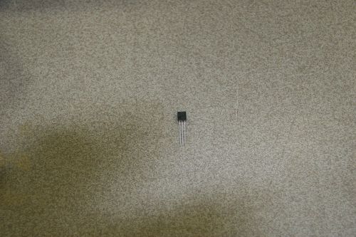
NTE ELECTRONICS P#PN2907A TRANSISTOR
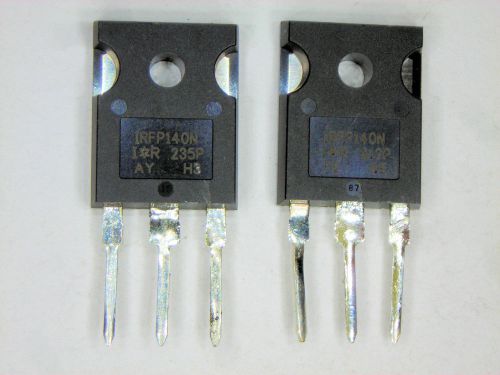
IRFP140N "Original" IR MOSFET Transistor 2 pcs
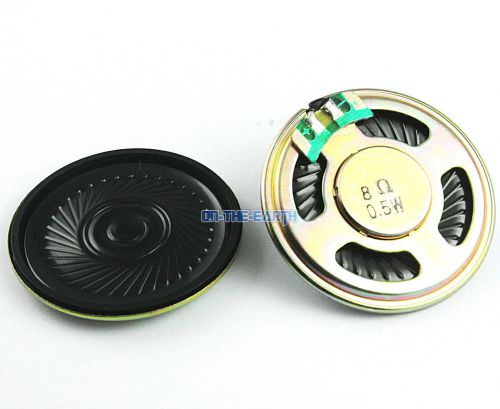
15 Pcs 40mm 0.5W 8 ohm Round Audio Speaker Loudspeaker
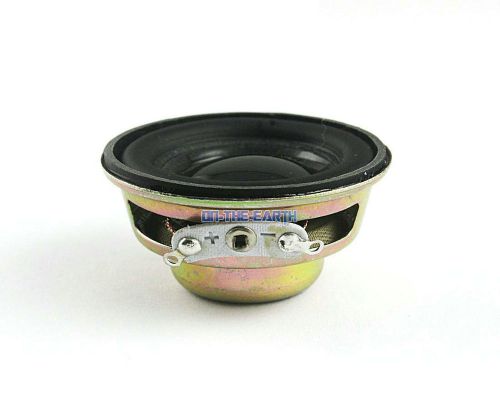
5 Pcs 40mm 3W 4 ohm Round Audio Speaker Loudspeaker
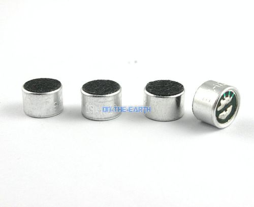
100 Pcs Mini 9x7mm 52db Electret Microphone Spy Condenser Pickup
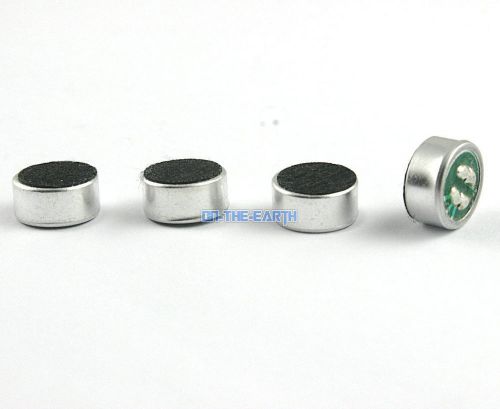
100 Pcs Mini 9x4.5mm 52db Electret Microphone Spy Condenser Pickup
By clicking "Accept All Cookies", you agree to the storing of cookies on your device to enhance site navigation, analyze site usage, and assist in our marketing efforts.
Accept All Cookies