
US $61.90
| Condition: |
New: A brand-new, unused, unopened, undamaged item in its original packaging (where packaging is
applicable). Packaging should be the same as what is found in a retail store, unless the item is handmade or was packaged by the manufacturer in non-retail packaging, such as an unprinted box or plastic bag. See the seller's listing for full details.
...
|
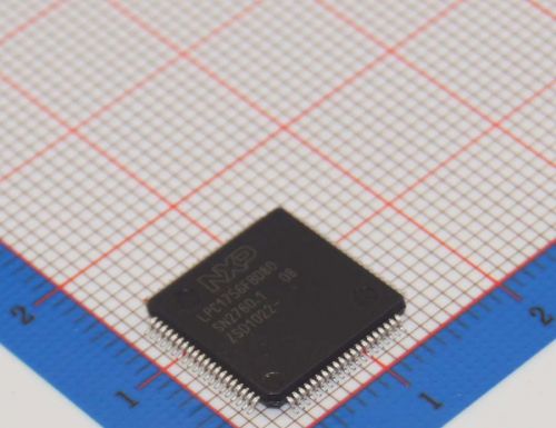
Brand | NXP |
| IC Package | LQFP80_12X12X05P | ||
| Model | GoJGo.com-10540 | ||
| Category | MCU | ||
| MPN | LPC1756FBD80 |
Directions
Similar products from Electrical Integrated Circuits & Processors
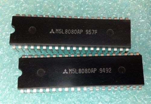
Motorola M5L8080AL CPU DIP Vintage Rare (US seller)
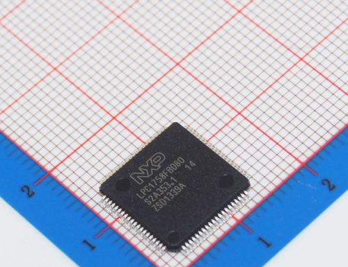
10 pcs/lot LPC1758FBD80, 32-bit ARM Cortex-M3 MCU, up to 512 kB flash
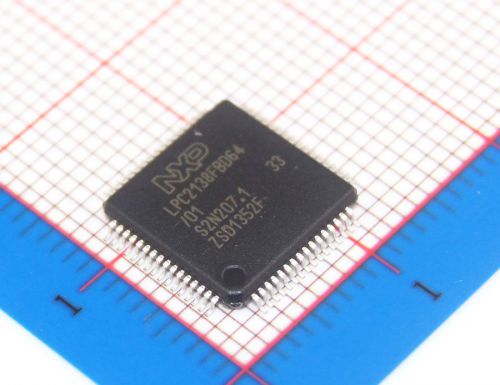
10 pcs/lot LPC2138FBD64, Single-chip 16/32-bit microcontrollers
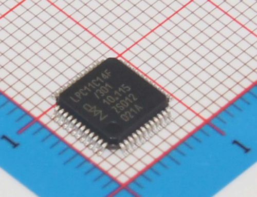
20 pcs/lot LPC11C14FBD48, 32-bit ARM Cortex-M0 microcontroller
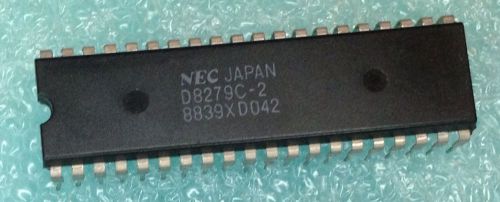
NEC D8279C-2 CPU DIP Vintage Rare (US seller)
Toshiba TMP8085AP CPU IC DIP Vintage Rare (US seller)
TA7642 Single AM Radio IC (Equivalent to ZN414) 2 pieces
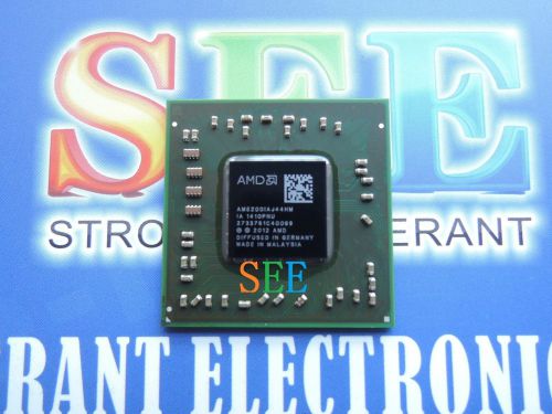
2pcs Original AMD AM5200IAJ44HM CPU DC:201410+
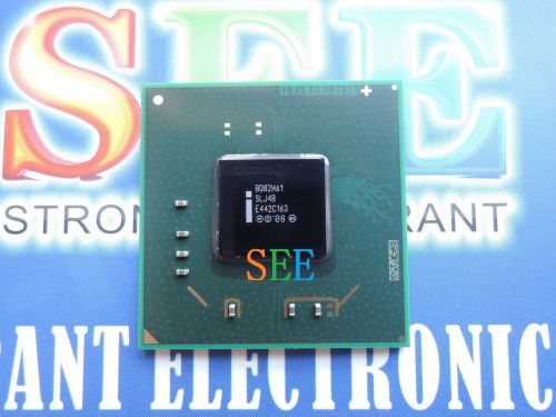
Original Intel BD82H61 SLJ4B Northbridge DC:201442+
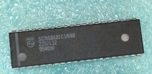
Phillips SCN68681C1N40 IC CPU DIP Vintage (US seller)
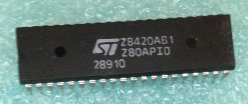
ST Z8420AB1 Z80APIO CPU DIP Vintage (US seller)

P8255A-5 AMD 40 PIN DIP Package Programmable Peripheral Interface NOS Vintage
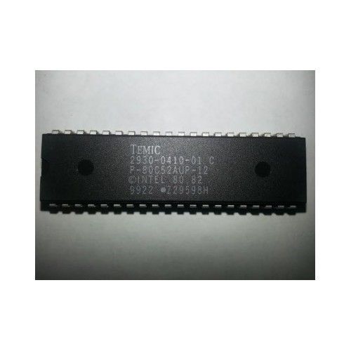
P80C52AUP INTEL 40 PIN DIP MICRO CONTROLLER-CPU PROCESSOR 8-BIT 12 MHz NOS
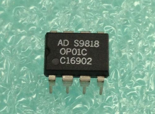
AD S9818 OP01C C16902 Analog Devices CPU DIP Vintage (US seller)
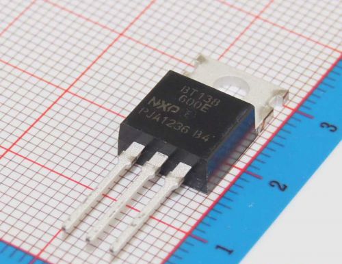
50 pcs/lot BT138-600E, 12 A four-quadrant triacs, sensitive gate
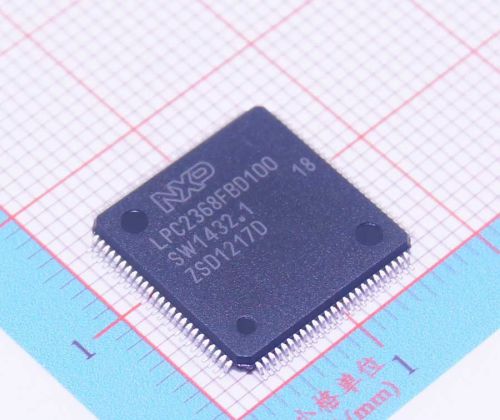
10 pcs/lot IC LPC2368FBD100, Single-chip 16-bit/32-bit microcontrollers
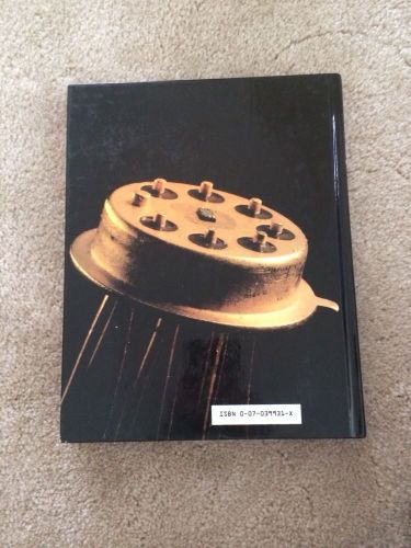
Operational Amplifiers and Linear Integrated Circuits Denton Dailey rare book
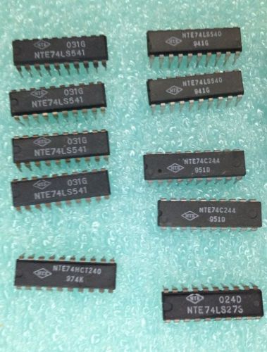
Lot of 25 NTE ICs (new) 74LS541 74LS540 74C244 74LS08 74LS11 74368 74LS21
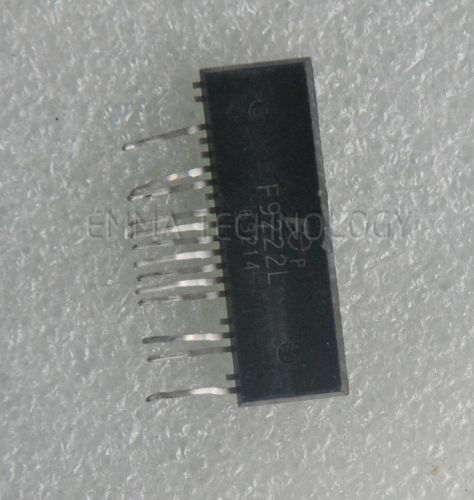
F9222L Manu:FUJI Encapsulation:ZIP-20,QUAD INVERTING TRANSISTOR SWITCH
People who viewed this item also vieved
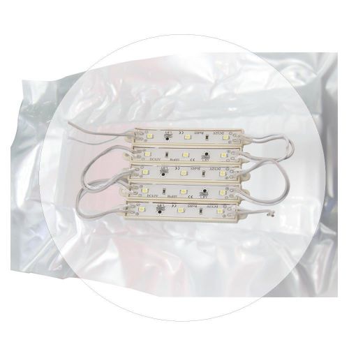
100pcs Waterproof LED Sign Module Light Lamp (SMD 3528,3LEDs,white light)
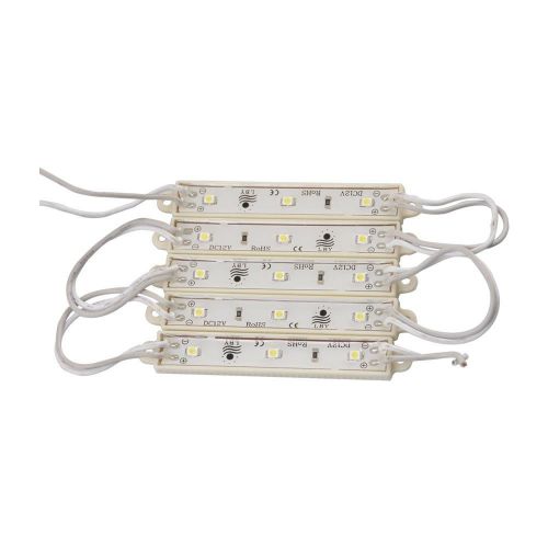
100 pcs Waterproof LED Sign Module Light Lamp (SMD 3528,3LEDs,white light)
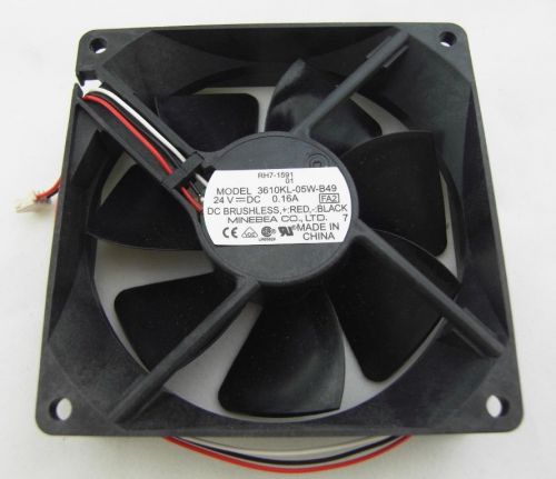
New NMB Cooling fan 3610KL-05W-B49 92*92*25MM 24V DC Fan
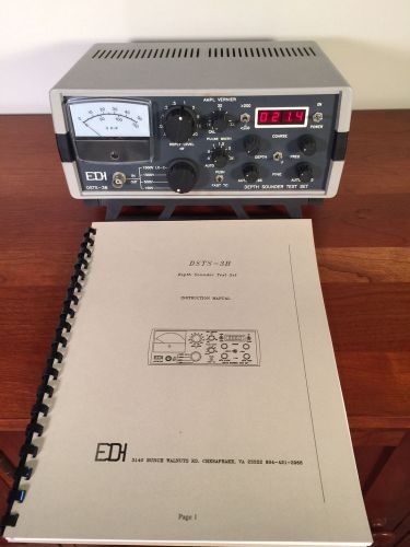
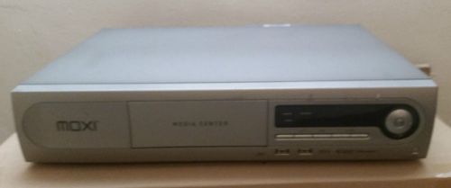
DSTS-3B Depth Sounder Test Set with manual
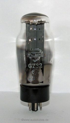
1 new tube Mullard 5V4G, CV 729, NOS (503022)
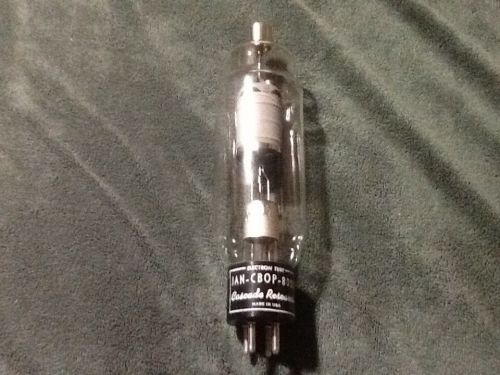
Vacuum Tube Cascade Research JAN CBOP 8020 FREE SHIPPING
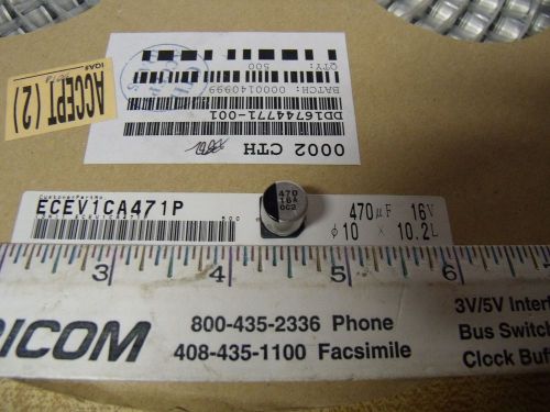
Capacitor SMT 470 uF at 16V Lot of 10
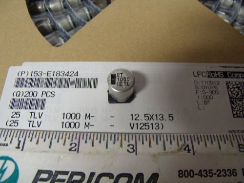
Capacitor SMT 1000 uF at 25V Lot of 10
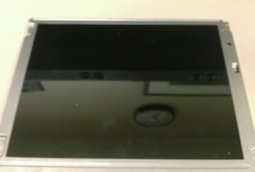
NEC ELO LCD Touchscreen Module Model NL8060BC26-27 ELO
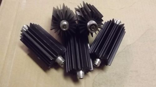
BIRD FIXED ATTENUATOR 25 WATTS 30 DB # 25-A-MFN-30
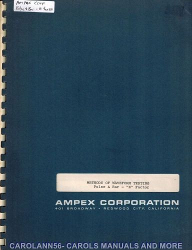
AMPEX CORP ABC Lab Report #26 METHODS OF WAVEFORM TESTING Pulse & Bar K Factor
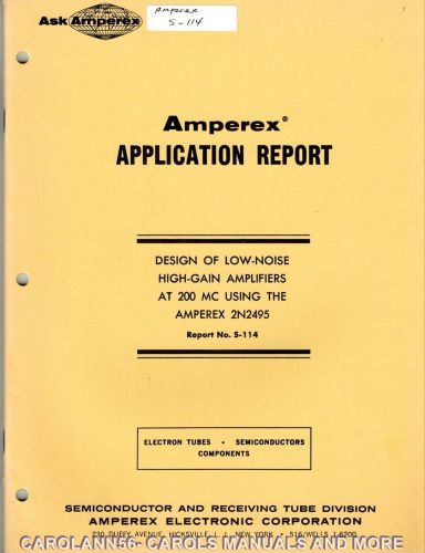
AMPEREX Application Report # S-114 Design of low-noise high-gain amplifiers
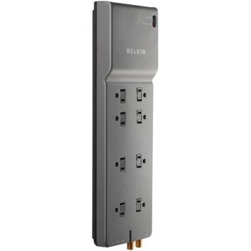
Belkin BE108230-12 Home/Office Surge Protector 8-Outlet 12ft Cord
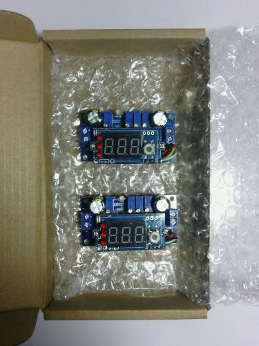
5 amp constant .mppt volt amp display lights Qty.2
By clicking "Accept All Cookies", you agree to the storing of cookies on your device to enhance site navigation, analyze site usage, and assist in our marketing efforts.
Accept All Cookies