US $18.88
| Condition: |
New: A brand-new, unused, unopened, undamaged item in its original packaging (where packaging is
applicable). Packaging should be the same as what is found in a retail store, unless the item was packaged by the manufacturer in non-retail packaging, such as an unprinted box or plastic bag. See the seller's listing for full details.
...
|
Brand | Unbranded/Generic |
| MPN | Does notapply | ||
| UPC | Does not apply |
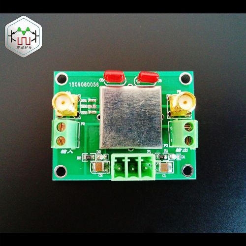
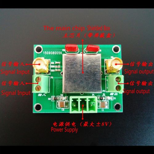
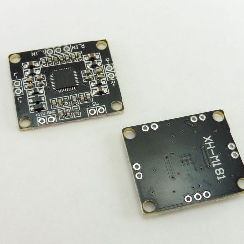
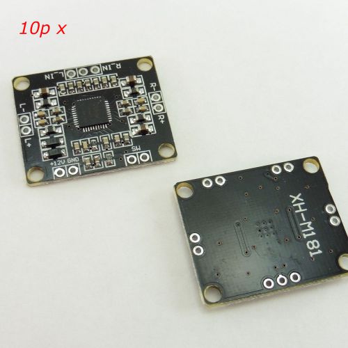
Directions
Similar products from Electric Audio Amplifiers & Module Boards
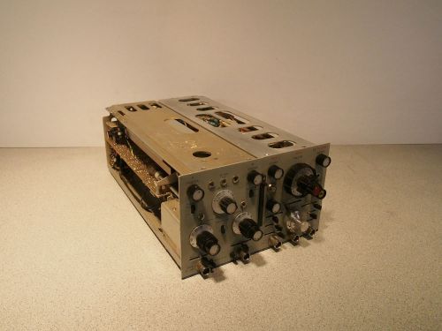
HP 1821A Time Base and Delay Generator w/ 1801A Dual Channel Vertical Amplifier
LM1036 + NE5532 Stereo Preamp Preamplifier Tone Board diy Amplifier 12V dc
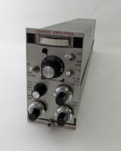
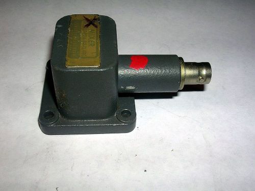
Unholtz-Dickie D22PMGS-HU Charge Amplifier
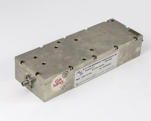
M/A-COM A1780-41/3963 Solid State Amplifier 3461258-1 SMA Female
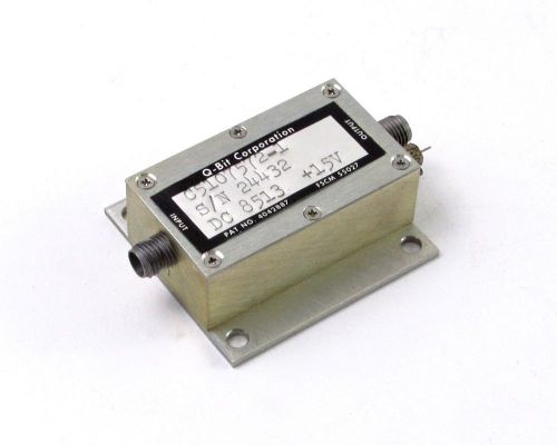
NEW - OLD STOCK Q-Bit C5107572-1 RF Amplifier - +15V, SMA Female
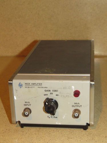
HEWLETT PACKARD 462A AMPLIFIER
TDA7293 x2pcs 170W Dual Parallel Mono Amplifier Board AMP Module Diy Kits
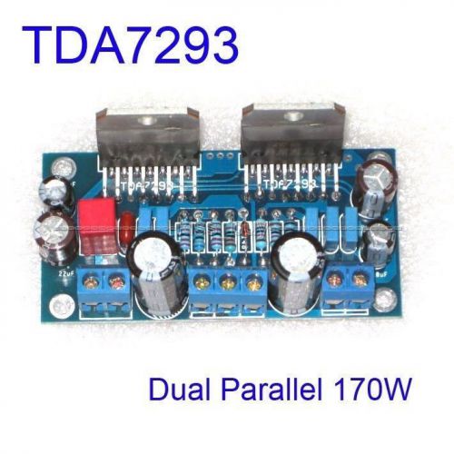
Assembled TDA7293 Dual Parallel 170W BTL Mono Audio Power Amplifier AMP Board
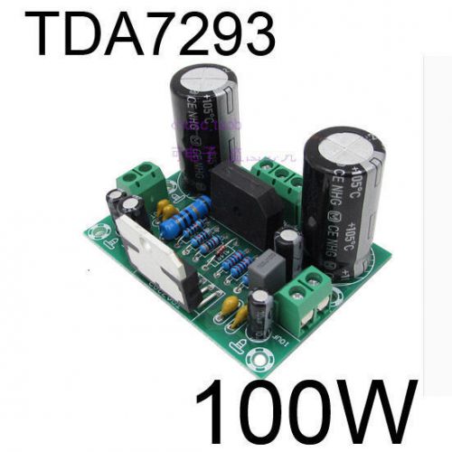
TDA7293 100W Mono Amplifier Board Double AC12~50V
TDA7293 x2 Dual Parallel 170W Mono Audio Power Amplifier AMP Board Diy Kits
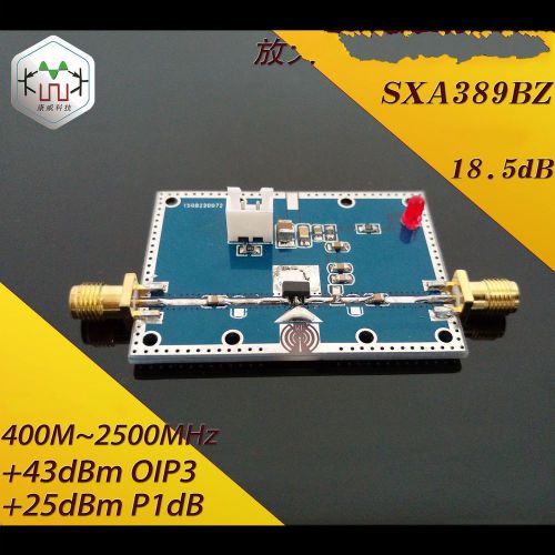
SXA-389B gain 18.5dB 400-2500MHz RF amplifier module single supply module
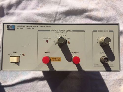
Agilent HP 11975A Amplifier 2.0- 8.0 GHz
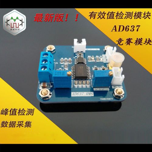
AD637 Peak Detection Signal Conditioning Peak RMS Detection Data Acquisition mod
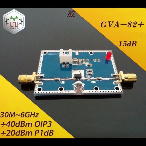
GVA-82 + 15dB Gain Amplifier RF Gain Blocks typical Single-supply Operation
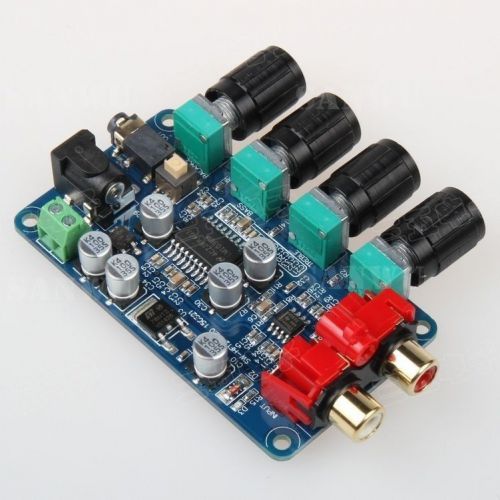
2PCS PAM8610 2*15W Dual channel Stereo Class Digital Amplifier Board 12V

5PCS PAM8610 2*15W Dual channel Stereo Class Digital Amplifier Board 12V
10PCS PAM8610 2*15W Dual channel Stereo Class Digital Amplifier Board 12V
2.1-GHz to 2.7-GHz 1-W Power Amplifier Eval Board TRF1123 TI
DC 12V TDA7297SA Stereo Two Channel 15W + 15W Amplifier Board No Noise
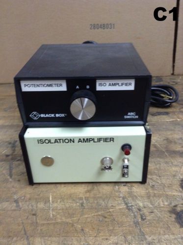
Black Box SW550A-BNC Isolation Amplifier-Grab Box of 2
People who viewed this item also vieved
SMA-CRC9 adapter RP-SMA Jack to CRC9 Plug Straight for huawei E16G E176G E169
N-UHF adapter N Jack to UHF PL259 plug Right Angle RF Coax Adapter connector
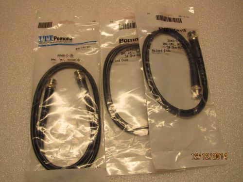
(2) Pomona 2249-C-24 BNC MALE-MALE CABLES & (1) POMONA 2249-C-36 BNC MALE-MALE
National Instruments NI SH68-68-EPM Shielded Cable, 1-Meter Length New in Bag
6x misc 50 ohm BNC terminators
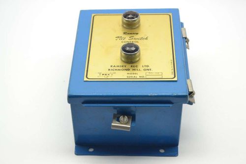
RAMSEY 20-35 TILT SENSOR 120V-AC 10A AMP CONTROLLER B396543
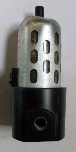
Wilkerson Series F Pneumatic Particulate Filter w/ Dent 1/4" F16-02-000 USG
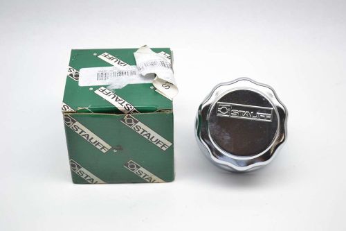
NEW STAUFF SMBT-80-S-40-0-N12-0 80 3/4 IN NPT METAL BREATHERS FILLER B430816
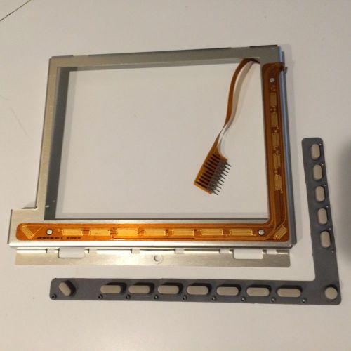
Tektronix 650-2927-00 Display Frame & Buttons for TDS Oscilloscope
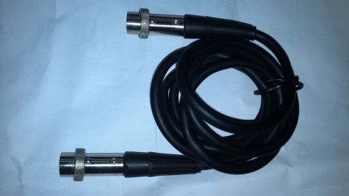
Canare 75 ohm Looping Plug (LP-1)
Agilent / HP E4808A High Performance Central Clock Module, 10.8 GHz Plug-in
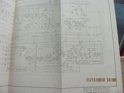
CUBIC MANUAL PN86-7300: Ohms Converter - Plug-In Accessory - O&M schem # 19436
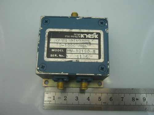
2 way AEL RF Power Divider 10-1000 MHz SMA 4dB insertion loss
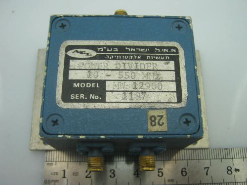
2 way AEL RF Power Divider 10-550 MHz SMA 4dB insertion loss
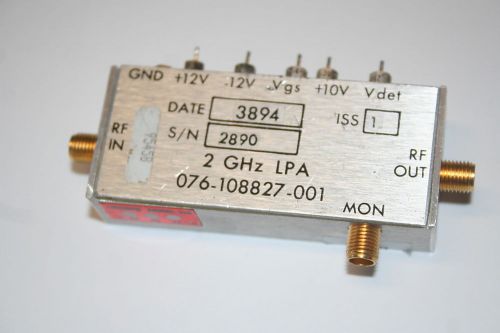
HARRIS 2 GHZ LPA MODULE ONLY 076-108827-001 EXCELLENT CONDITION SMA
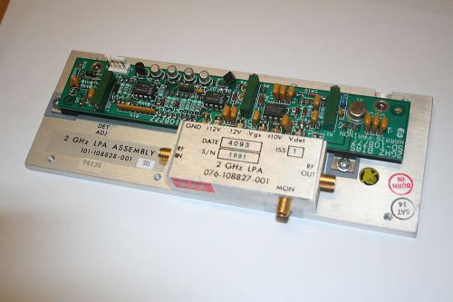
HARRIS FARINON 2 GHz LPA ASSEMBLY, 101-108828-001, 076-108827-001 w/ 2 GHZ BIAS
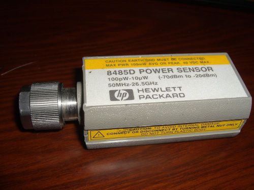
Agilent / HP 8485D Power Sensor **TESTED** 50 MHz to 26.5 GHz -20 to -70 dBm
Cable assy for Boonton RF Probe and Boonton Power Sensor
HP AGILENT 11521A MIXER WR90-BNC 8.2- 12.4GHz.
TRG A520/69 VARIABLE ATTENUATOR WR 28 26.5-40 GHz.
IC SMD Vacuum Sucking Pen Sucker Pick Up Hand + 4 Suction Headers MT-668
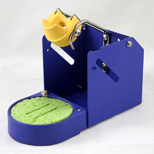
Hakko FH200-51 Holder w/Sponge for FM-2032, FM-206/203, FX-951, FH-200
By clicking "Accept All Cookies", you agree to the storing of cookies on your device to enhance site navigation, analyze site usage, and assist in our marketing efforts.
Accept All Cookies